Views: 0 Author: Site Editor Publish Time: 2026-08-04 Origin: Site


Electronic connectors function as the indispensable interface that enables signal and power transmission between separate circuit boards, modules, and subsystems across virtually every electronic device in operation today. From consumer smartphones to automotive control units, industrial automation equipment to telecommunications infrastructure, these components ensure that electrical pathways remain stable and reliable under a wide spectrum of operating conditions. The manner in which they are produced directly governs their electrical performance, mechanical durability, and long-term field reliability.
The production sequence behind these compact components involves a convergence of precision engineering, material science, and automated manufacturing technologies. Each connector type follows a multi-stage pipeline that converts raw metals and engineering plastics into finished, tested interconnect solutions.
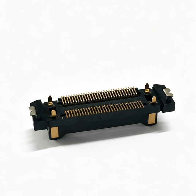
The Connector Manufacturing Process encompasses a series of coordinated production stages including product design, tooling development, contact stamping, surface plating, housing molding, automated assembly, and rigorous quality testing, all working together to transform raw metals and plastics into reliable interconnection devices that meet precise electrical and mechanical specifications.
Understanding how connectors are produced offers valuable context for design engineers, procurement specialists, and product managers. The production methodology influences unit cost, delivery timelines, and critical performance parameters such as contact resistance, insertion force, and environmental resilience. By examining each manufacturing stage in detail, readers can better evaluate the engineering decisions that determine connector quality.
The sections that follow break down the entire production workflow from initial concept to final packaging, covering the technical considerations, material selections, and quality benchmarks that define modern connector manufacturing.

Table of Contents
This multi-stage production system transforms raw materials such as copper alloys, engineering thermoplastics, and precious metals into finished electronic connectors through sequential operations encompassing design, stamping, plating, molding, assembly, and testing.
At its core, this pipeline represents a carefully orchestrated sequence of manufacturing operations, each contributing specific attributes to the final product. The workflow begins with raw material preparation, where copper alloy strips and plastic resins are sourced to precise specifications. These materials pass through stamping presses that shape metal into contacts, plating lines that apply protective surface finishes, and molding machines that form insulating housings. The contacts and housings converge at the assembly stage, where automated equipment inserts, secures, and tests each unit before packaging.
The complexity of this sequence varies significantly depending on connector type. A simple pin header may require only basic stamping, tin plating, and manual assembly, while a high-density board-to-board connector may involve ultra-precision stamping, selective gold plating, multi-cavity molding, and fully automated assembly with vision system verification.
The materials selected at the design stage fundamentally shape the manufacturing approach. The following table summarizes the primary material categories used in interconnect production and their respective roles:
Material Category | Common Types | Primary Function |
|---|---|---|
Contact Base Metal | Phosphor bronze, brass, copper alloy | Electrical conductor and spring mechanism |
Plating Material | Gold, tin, palladium, silver | Surface protection and contact reliability |
Housing Polymer | LCP, nylon, PCT, PPS | Insulation and mechanical structure |
Auxiliary Materials | Solder paste, adhesives, packaging media | Assembly aid and protection |
Each material category interacts with specific manufacturing stages. The base metal formability dictates stamping parameters, the plating material chemistry determines bath composition and process duration, and the polymer flow characteristics influence molding temperature and pressure settings. Material selection therefore serves as a foundational decision that cascades through every subsequent production operation.
The design and engineering phase establishes the complete technical specification of a connector, including contact geometry, material selection, dimensional tolerances, and performance targets, serving as the foundational blueprint for all subsequent manufacturing operations.
Every connector begins as a concept driven by an application requirement. Design engineers define electrical parameters such as current rating, signal frequency, and contact resistance, alongside mechanical parameters including pitch, pin count, stacking height, and mating cycle target. These specifications are translated into preliminary CAD models that visualize the contact shape, housing structure, and overall connector footprint.
The design phase increasingly relies on simulation tools to predict performance before any physical prototype is produced. Electrical simulation verifies signal integrity, while mechanical finite element analysis evaluates contact force distribution and stress concentrations under repeated mating cycles. These virtual validation steps reduce physical iterations and lower tooling investment risk.
Material selection during the design phase directly determines which manufacturing processes will be required. The contact base metal must balance electrical conductivity with mechanical spring properties. Phosphor bronze is widely favored for its excellent elastic recovery and corrosion resistance, making it suitable for contacts that undergo repeated mechanical stress. Brass offers higher conductivity at lower cost but exhibits inferior spring characteristics.
Plating specifications defined during design specify not only the plating material but also the thickness, coverage area, and application method. Gold plating thickness may range from 0.05 micrometers for cost-sensitive consumer applications to 0.75 micrometers or more for automotive and industrial environments requiring extended durability. Selective plating, where precious metal is applied only to the contact interface while the tail portion receives tin plating for solderability, represents a common strategy to balance performance with material cost.
The final design output consists of a complete set of engineering drawings and specifications that define every dimensional tolerance, surface finish requirement, and material callout. Typical tolerance bands for connector contacts fall within 0.02 to 0.05 millimeters for critical forming dimensions. The following list highlights key parameters finalized during this phase:
Contact beam geometry and deflection range
Normal force at the contact interface (typically 30 to 200 grams per contact)
Insertion and extraction force limits
Dielectric withstanding voltage
Insulation resistance between adjacent contacts
Operating temperature range
Mating cycle durability target
Once these specifications are frozen, the design is released to the tooling and production teams, marking the transition from engineering to physical manufacturing. The thoroughness of the design phase directly correlates with the smoothness of subsequent production operations.

The stamping process uses precision progressive dies installed in high-speed presses to cut, form, and bend metal strips into connector contacts with exact dimensional accuracy, creating the conductive elements that carry electrical signals between mating connector halves.
This forming operation begins with the design and construction of progressive dies, which are multi-station tooling assemblies that perform a sequence of cutting and forming operations as the metal strip advances through the die. Each station performs a specific operation such as piercing, blanking, bending, coining, or shearing. A typical connector contact die may contain 15 to 40 stations, progressively transforming a flat metal strip into a three-dimensional contact with complex beam geometry, tail features, and retention barbs.
Die construction demands extremely tight machining tolerances, often measured in micrometers, because any dimensional variation in the die transfers directly to the stamped product. Die components are typically fabricated from tool steel or tungsten carbide, with carbide preferred for high-volume applications due to its superior wear resistance.
During production, the stamping press operates at speeds ranging from 200 to 1,200 strokes per minute depending on part complexity and tolerance requirements. The metal strip, typically supplied in coil form with thickness between 0.1 and 0.5 millimeters, is fed into the die via a servo-controlled feeder. Lubricants are applied to reduce friction and prevent galling, though these must be compatible with subsequent plating operations.
Quality monitoring during stamping has evolved with in-die sensing technology. Force sensors detect anomalies such as slug pulling, misfeeds, or broken punches, triggering automatic press shutdown. The following table summarizes key stamping parameters:
Parameter | Typical Range | Impact on Quality |
|---|---|---|
Press Speed | 200 to 1200 SPM | Affects form accuracy and tool wear |
Material Thickness | 0.10 to 0.50 mm | Determines contact stiffness and current capacity |
Dimensional Tolerance | 0.02 to 0.05 mm | Governs mating performance and reliability |
Coil Width | 12 to 80 mm | Matches die design and part layout |
Burr Height | Below 0.02 mm | Influences plating coverage and insertion force |
After stamping, contact strips may be collected in carrier strips for reel-to-reel plating or singulated for batch processing depending on the plating method selected. The stamped contacts at this stage are functional but lack the surface protection necessary for reliable long-term operation. The burr direction, edge quality, and dimensional consistency established during stamping directly influence plating coverage uniformity and ultimately the electrical performance of the finished connector.
The plating process applies thin layers of noble or semi-noble metals onto stamped contacts to provide corrosion resistance, reduce contact resistance, and ensure long-term electrical reliability across thousands of mating cycles in diverse environmental conditions.
Plating for connector contacts is predominantly performed using reel-to-reel continuous plating or batch barrel plating. Reel-to-reel plating, the more common approach for high-volume production, feeds the stamped contact carrier strip continuously through a series of plating baths. This method enables selective plating, where different contact zones receive different finishes. For example, the mating interface may receive gold plating while the solder tail receives tin plating, optimizing both performance and material cost. Batch plating processes singulated contacts in rotating baskets and is typically used for lower-volume parts.
Regardless of method, the plating line begins with a thorough cleaning sequence to remove stamping lubricants, oxides, and particulate contamination. This typically involves alkaline degreasing, ultrasonic cleaning, acid activation, and multiple deionized water rinses. Surface cleanliness is critical because any residual contamination disrupts plating adhesion and uniformity.
The choice of plating material is driven by the application environment, cost targets, and performance requirements. Gold remains the premium choice for contact interfaces due to its exceptional corrosion resistance and consistently low contact resistance. Tin plating is widely used for solderable tails and lower-cycle contacts due to its low cost and good solderability. Palladium and palladium-nickel alloys, often overplated with a thin flash of gold, offer a cost-effective middle ground with excellent durability.
Plating Material | Typical Thickness | Key Properties | Common Application |
|---|---|---|---|
Hard Gold | 0.05 to 0.75 micrometers | Excellent corrosion resistance, low contact resistance | High-reliability contact interfaces |
Tin (Matte or Bright) | 1.0 to 3.0 micrometers | Good solderability, economical | Solder tails, consumer-grade contacts |
Palladium-Nickel with Gold Flash | 0.2 to 0.5 micrometers | High durability, cost-effective alternative to thick gold | Automotive and telecom contacts |
Silver | 1.0 to 5.0 micrometers | High conductivity, suitable for high current | Power connectors |
Plating quality is verified through process monitoring and post-plating inspection. X-ray fluorescence instruments measure plating thickness at specified locations on the contact. Salt spray testing, porosity testing, and adhesion tape testing validate the plating ability to withstand environmental exposure. Surface finishing is one of the most tightly controlled stages in production because plating defects such as voids, thin spots, or poor adhesion directly translate into elevated contact resistance and intermittent electrical failures.
Nearly all gold-plated contacts receive a nickel underplate layer, typically 0.5 to 2.0 micrometers thick, between the base metal and the precious metal top layer. The nickel underplate serves as a diffusion barrier that prevents base metal elements from migrating through the gold layer and oxidizing at the surface. It also provides a hard, smooth substrate that enhances the durability of the gold layer under mechanical wear. Omitting the nickel underplate is a common cost reduction shortcut that significantly reduces contact reliability and is generally avoided in quality-focused production.

Injection molding produces the plastic housings and insulators that hold connector contacts in precise alignment, using engineering thermoplastics such as LCP, PA, or PCT to provide electrical insulation, mechanical protection, and dimensional stability across operating temperature ranges.
The molding operation for connector housings begins with mold design, which must accommodate features such as contact cavities, alignment ribs, locking mechanisms, and polarization features. Multi-cavity molds, often containing 4 to 32 cavities, are standard for high-volume production. The mold includes precision-machined core and cavity inserts, cooling channels, and ejection mechanisms, all designed to produce parts with dimensional tolerances as tight as 0.02 millimeters.
Mold flow analysis software is routinely employed to simulate plastic flow, predict potential defects, and optimize gate placement and cooling channel layout. This simulation-driven approach reduces the number of mold trials needed.
During production, the molding machine melts the thermoplastic resin and injects it into the mold cavity under precisely controlled temperature and pressure profiles. Melt temperatures typically range from 280 to 360 degrees Celsius, with injection pressures of 600 to 1,500 bar. Cycle times for connector housings generally range from 8 to 30 seconds depending on part size and material characteristics.
The choice of thermoplastic material significantly influences the molding parameters and finished housing performance. Liquid Crystal Polymer (LCP) is favored for high-density connectors due to its exceptional flow characteristics that enable filling of thin-wall sections as narrow as 0.15 millimeters. Polyamide (nylon) provides excellent mechanical toughness for larger housings. PCT offers superior thermal stability for connectors undergoing lead-free reflow soldering at peak temperatures exceeding 260 degrees Celsius.
After molding, housings undergo inspection for flash, short shots, sink marks, and dimensional compliance. Critical dimensions such as contact cavity diameter, pitch accuracy, and overall housing flatness are verified using optical measurement systems. Housings that pass inspection are then staged for the assembly operation. The quality of the molded housing directly affects assembly yield and final connector performance, as even minor dimensional deviations can cause contact misalignment, inconsistent mating force, or insufficient contact normal force.
The assembly stage integrates stamped and plated contacts into molded housings using automated insertion equipment, followed by packaging operations that prepare finished connectors for shipment in formats compatible with customer assembly processes.
Assembly lines for connector production typically utilize automated insertion machines that pick individual contacts from a carrier strip or bowl feeder and insert them into the molded housing at precisely controlled positions and forces. The insertion process must overcome the housing cavity interference fit while ensuring that the contact retention feature engages securely. Improper insertion can damage the contact beam or result in incomplete seating that causes intermittent connections.
For high-pin-count connectors, multi-head insertion machines process multiple contacts simultaneously. Vision systems verify contact presence, orientation, and insertion depth after each cycle. The following list outlines the key assembly operations:
Contact singulation and orientation
Automated insertion with force monitoring
Retention verification through optical or mechanical probing
Mating and unmating force testing on sampled units
Lid or cover attachment for enclosed connector types
Laser marking or label application for part identification
Finished connectors are packaged in formats that align with the customer assembly process. Surface-mount connectors are typically supplied in tape and reel packaging, where individual connectors are sealed in pocketed carrier tape with a protective cover film and wound onto reels. Through-hole connectors may be packaged in tubes or trays depending on pin count and body size. The following table compares common packaging formats:
Format | Typical Application | Advantages |
|---|---|---|
Tape and Reel | Surface-mount connectors | Compatible with automated pick-and-place equipment |
Tube | Through-hole pin headers and sockets | Cost-effective for larger body sizes |
Tray | High-pin-count or fragile connectors | Protects delicate features during handling |
Bulk | Low-cost commodity connectors | Minimal packaging cost for manual assembly |
Each packaging format must maintain connector orientation and protect contacts from mechanical damage during transit. Moisture-sensitive components may require vacuum-sealed bags with desiccant to prevent moisture absorption during reflow soldering.

Quality assurance in connector production involves a comprehensive system of dimensional inspection, electrical testing, mechanical cycling, and environmental validation to verify that every production lot meets applicable specifications and industry standards.
Dimensional inspection throughout the production process ensures that contacts, housings, and assembled connectors conform to engineering tolerances. Optical measurement systems and vision-based inline inspection stations capture critical dimensions at high frequency, generating statistical process control data. Visual inspection criteria address surface defects such as plating voids, flash, burrs, and deformation.
Electrical testing validates the functional performance of finished connectors. Contact resistance measurements, typically specified at 20 milliohms or below for signal contacts, confirm that plating quality and contact geometry deliver the expected conductivity. Dielectric withstanding voltage testing verifies insulation integrity, while insulation resistance testing confirms that leakage current between contacts remains within specified limits.
Mechanical testing evaluates the connector ability to withstand physical stresses. Mating and unmating force testing measures the force required to engage and disengage the connector. Durability cycling subjects sample connectors to repeated mating cycles, often 50 to 1,000 depending on specification, to verify that contact force and resistance remain stable over the rated cycle life.
Environmental testing simulates the conditions connectors will encounter in their intended applications. The following table outlines common test categories and their purposes:
Test Category | Standard Reference | Purpose |
|---|---|---|
Thermal Cycling | EIA-364-32 | Evaluate performance across temperature extremes |
Humidity Exposure | EIA-364-31 | Assess corrosion resistance under moisture |
Salt Spray | ASTM B117 | Validate plating protection in corrosive environments |
Vibration and Shock | EIA-364-28 | Verify mechanical integrity under dynamic stress |
Current Cycling | EIA-364-70 | Assess thermal-mechanical fatigue from power cycling |
These tests are typically performed on samples from each production lot, with results documented in certificates of compliance provided to customers. The rigor of the testing program directly correlates with the reliability of connectors in field service, making quality assurance an integral component of the production workflow rather than an optional add-on.
The connector industry is evolving through miniaturization demands, higher data rate requirements, automation advancements, and sustainable material innovations that are reshaping how connectors are designed, produced, and validated.
The relentless trend toward smaller, lighter, and more functional electronic devices drives connector manufacturers to develop contacts and housings at ever-decreasing pitches. Connector pitches of 0.4 millimeter and below are now common in mainstream consumer electronics. This miniaturization challenges every stage of the production chain, requiring tighter stamping tolerances, more precise molding capabilities, and more sensitive inspection equipment. Stamping must produce contacts with beam widths measured in tens of micrometers, while molding must fill wall sections approaching 0.1 millimeter without defects.
Simultaneously, the demand for higher data rates pushes connector designs toward impedance-controlled architectures that maintain signal integrity at frequencies exceeding 25 gigabits per second per lane.
Manufacturing automation continues to advance, with fully integrated production lines that link stamping, plating, molding, and assembly under unified process control. Real-time data collection enables predictive maintenance, process optimization, and traceability from raw material to finished product. Machine vision systems powered by artificial intelligence are increasingly deployed for defect detection.
Environmental considerations are influencing material selection and process design across the connector industry. Lead-free plating chemistries, halogen-free housing materials, and energy-efficient production equipment are becoming standard. Some manufacturers are exploring recycled polymer content and closed-loop water systems. These initiatives must be balanced against performance and reliability requirements, creating new engineering challenges across the production pipeline.
Connector contacts are typically stamped from copper alloys such as phosphor bronze or brass. Contact surfaces are plated with gold, tin, or palladium to provide corrosion resistance and reliable electrical contact. Housings are produced from engineering thermoplastics including LCP, nylon, and PCT.
The timeline from initial design to volume production typically spans 8 to 20 weeks depending on connector complexity. Tooling fabrication for progressive dies and injection molds accounts for the longest segment, often requiring 6 to 12 weeks. First article inspection and qualification testing add another 2 to 4 weeks.
Stamping determines the dimensional accuracy and mechanical properties of connector contacts. Variations in contact geometry directly affect normal force, contact resistance, and mating durability. Because subsequent plating and assembly operations depend on consistent stamping quality, any deviation propagates through the entire production pipeline.
Plating applies a protective and conductive surface layer that prevents base metal oxidation, reduces contact resistance, and provides mechanical wear resistance. Without adequate plating, copper alloy contacts would oxidize rapidly, causing unstable contact resistance and eventual signal or power interruption. Gold plating offers the highest reliability, while tin plating provides a cost-effective solution for lower-cycle applications.
The molding operation produces the housing that maintains precise contact alignment, provides electrical insulation, and contributes to the mechanical robustness of the connector assembly. Housing dimensional accuracy directly influences contact position, mating force consistency, and the connector ability to withstand shock and vibration.