Views: 0 Author: Site Editor Publish Time: 2026-07-17 Origin: Site


Table of Contents
The transition to PCIe Gen 5.0, Gen 6.0, and the upcoming Gen 7.0 has transformed the physical interface from a simple mechanical slot into a highly sensitive component in high-speed PCB design. As data rates scale aggressively to 32 GT/s, 64 GT/s, and 128 GT/s, hardware engineers face shrinking signal integrity margins. Improper component selection or suboptimal layout routing directly leads to severe signal degradation, compliance failures, and board respins. Modern hardware architecture requires a rigorous approach to physical interconnects. A PCIe connector must handle advanced modulation schemes while maintaining strict impedance control. This guide provides hardware engineers and system architects with an evidence-based framework for evaluating, selecting, and implementing the optimal interface based on form factor constraints, electrical performance requirements, and PCI-SIG compliance standards. You will learn how to match mechanical footprints to spatial constraints and apply routing strategies that mitigate parasitic losses.
Generational Tolerance: PCIe Gen 5 and Gen 6 connectors require significantly tighter tolerances for insertion loss and crosstalk due to the shift to PAM4 signaling and higher Nyquist frequencies.
Form Factor Alignment: Selecting between CEM, M.2, U.2, or MCIO depends strictly on the application's spatial constraints, thermal management capabilities, and peripheral type (e.g., GPU vs. NVMe storage).
Routing Realities: Successful implementation relies heavily on mitigating via parasitics, maintaining strict 85-ohm or 100-ohm differential impedance, and adhering to specific length-matching rules for data lanes versus clock signals.
Total Cost of Implementation: Over-specifying a connector (e.g., Gen 6 for a Gen 4 application) increases BOM costs unnecessarily, while under-specifying introduces fatal bit error rates (BER).
Understanding how bandwidth scaling dictates physical requirements ensures future-proof hardware designs. System architects must evaluate how each generational leap alters the physical layer constraints and electrical performance demands placed on the board-level interconnects. The jump from one generation to the next is no longer just a matter of swapping a silicon controller; it requires a complete re-evaluation of the PCB stack-up, trace routing, and the mechanical interface itself.
PCIe Gen 4 operates at 16 GT/s using Non-Return-to-Zero (NRZ) signaling. It serves as the baseline for modern enterprise and consumer hardware. At this speed, engineers can maintain manageable signal integrity margins using standard FR4 materials and well-optimized through-hole connectors, provided trace lengths remain relatively short. The Nyquist frequency sits at 8 GHz, which allows for some leniency in via design and connector pad geometries.
Gen 5 doubles the throughput to 32 GT/s while retaining NRZ signaling. This frequency jump drastically reduces the allowable loss budget. Implementing a Gen 5 PCIe connector requires advanced PCB materials like Megtron 6, Tachyon, or similar low-loss laminates. You must strictly optimize connector footprints to minimize reflection, often mandating surface-mount technology (SMT) over traditional press-fit or through-hole options to eliminate via stubs. The 16 GHz Nyquist frequency means that even a 10-mil via stub can act as a resonant antenna, destroying the signal eye.
Gen 6 pushes the boundary to 64 GT/s by introducing Pulse Amplitude Modulation 4-level (PAM4), Forward Error Correction (FEC), and FLIT mode. PAM4 transmits two bits per clock cycle, which degrades the signal-to-noise ratio (SNR) significantly compared to NRZ. The voltage margin between states drops by roughly a factor of three. This standard demands ultra-low crosstalk connectors and highly controlled impedance environments. Even minor impedance discontinuities at the connector interface will cause unacceptable bit error rates. The mechanical tolerances for the pins inside the connector housing must be exceptionally tight to prevent intra-pair skew.
PCIe Generation | Data Rate | Signaling Type | Nyquist Frequency | Typical PCB Material |
|---|---|---|---|---|
Gen 4 | 16 GT/s | NRZ | 8 GHz | Mid-loss (e.g., Megtron 4) |
Gen 5 | 32 GT/s | NRZ | 16 GHz | Ultra-low loss (e.g., Megtron 6) |
Gen 6 | 64 GT/s | PAM4 | 16 GHz | Ultra-low loss + strict weave |
Gen 7 | 128 GT/s | PAM4 | 32 GHz | Next-gen laminates / Twinax |
PCIe Gen 7.0 targets 128 GT/s, scaling further via PAM4 signaling and FLIT mode. The integration of AXI system-level interfaces heavily impacts controller throughput demands, forcing the physical layer to handle unprecedented data density. At 128 GT/s, the Nyquist frequency reaches 32 GHz, where copper trace attenuation becomes a massive hurdle. Skin effect and dielectric loss dominate the channel characteristics at these frequencies.
This reality is driving a rapid evolution in interface design. We are seeing a transition toward optical or near-packaged optic interfaces and ultra-low-loss copper twinax cables to handle extreme physical-layer attenuation. Board-to-board connections will likely rely more on specialized cabling solutions rather than traditional edge-card slots to bypass the lossy PCB materials entirely. The traditional edge connector may become obsolete for long-reach channels in Gen 7 architectures.
Mechanical compatibility across generations remains a core tenet of the PCI-SIG specifications, but electrical performance limitations dictate actual system capabilities. A Gen 5 card will physically fit into a Gen 3 slot, but the host system will auto-negotiate the link down to the lowest common denominator. The link training and status state machine (LTSSM) handles this negotiation during the boot sequence.
Mating legacy cards with high-speed host connectors carries minimal risk, but placing a high-speed Gen 5 card into a legacy Gen 3 or Gen 4 slot can introduce unexpected signal reflections if the older connector lacks the necessary impedance control. Engineers must ensure the physical interface matches the intended operational bandwidth to avoid bottlenecking the entire system architecture. You cannot simply drop a high-speed ASIC onto a board with legacy connectors and expect it to pass compliance testing.
Categorizing connectors by mechanical footprint and primary application use cases helps narrow down the selection process. The physical envelope of the end product dictates which form factor is viable. You must balance board real estate, thermal airflow, and mechanical retention requirements.
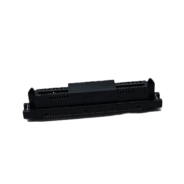
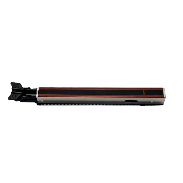
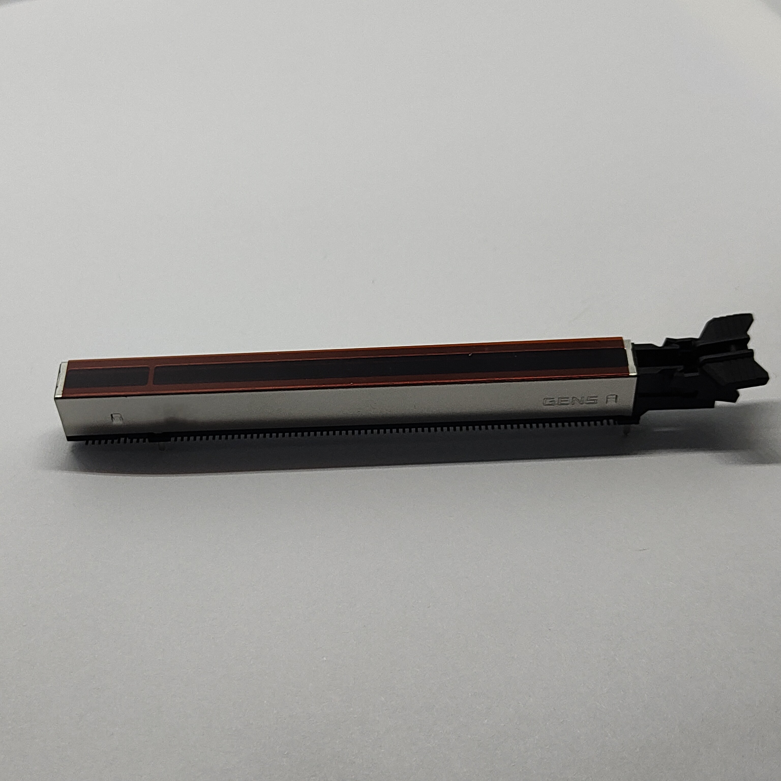
The CEM specification defines the standard motherboard slot. These come in x1, x4, x8, and x16 lane configurations, dictating the standard add-in card mechanical dimensions. You will find CEM slots primarily used for Graphics Processing Units (GPUs), high-performance network interface cards (NICs), and heavy hardware accelerators. The CEM form factor is the backbone of desktop and workstation architectures.
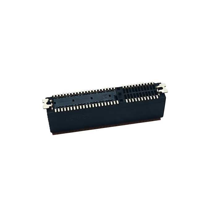
When evaluating CEM options, engineers must choose between through-hole technology (PTH), surface mount technology (SMT), and press-fit mounting. PTH provides excellent mechanical retention for heavy cards but introduces via stubs that degrade high-speed signals. SMT offers superior signal integrity by keeping the signal on the surface layer or utilizing microvias, but it sacrifices some mechanical strength, often requiring additional retention brackets. Press-fit is common in thick server backplanes but requires specialized tooling and careful consideration of the plated through-hole (PTH) tolerances.
M.2 connectors dominate compact designs. They sit parallel to the board, offering extreme spatial efficiency in dense server or mobile designs. Common applications include solid-state drives (SSDs), Wi-Fi/Bluetooth modules, and cellular modems. You must specify the correct keying type (M-key, B-key, E-key) to ensure mechanical compatibility with the target peripheral. The M.2 specification also dictates specific component height limits on both the top and bottom of the module.
U.2 and U.3 connectors serve the enterprise storage market. They allow NVMe drives to utilize the familiar 2.5-inch form factor while routing PCIe lanes directly to the drive. These connectors are built for hot-swapping and high mating cycles, making them ideal for server storage backplanes. U.3 specifically allows for tri-mode operation, supporting NVMe, SAS, and SATA drives in the same physical slot, which drastically simplifies backplane design for storage arrays.
Rigid PCB routing is often unfeasible in modular compute architectures and dense server chassis. High-speed internal cabling solutions like MCIO (Mini Cool Edge IO), OCuLink, and Mini-SAS HD bridge the gap between motherboards and peripheral backplanes. These connectors allow you to route high-speed signals over longer distances without paying the penalty of expensive low-loss PCB materials across a massive motherboard.
These cable assemblies bypass the lossy PCB traces. When evaluating these options, compare the cable assembly insertion loss against the board-to-board connector loss. In Gen 5 and Gen 6 systems, routing signals through a twinax MCIO cable often yields better signal integrity over a 15-inch run than routing through premium PCB laminates. The twinax cable provides a highly controlled dielectric environment and excellent shielding against external EMI.
Vetting supplier datasheets against actual design requirements prevents late-stage compliance failures. You must evaluate electrical, mechanical, and certification parameters simultaneously. Relying solely on a marketing datasheet without reviewing the S-parameters is a guaranteed path to failure.
Electrical performance dictates whether the link will establish and maintain the target bandwidth. Focus on these specific metrics when reviewing the component specifications:
Insertion Loss & Return Loss: Verify the acceptable dB thresholds at the target Nyquist frequencies. For Gen 5, check the loss at 16 GHz. For Gen 6, check 32 GHz. High return loss indicates an impedance mismatch within the connector housing.
Crosstalk (NEXT & FEXT): Near-end and far-end crosstalk isolation requirements between adjacent differential pairs are critical, especially in dense x8 and x16 configurations. High crosstalk shrinks the PAM4 eye diagram instantly, leading to link degradation.
Impedance Control: Match the connector's native impedance to your PCB stack-up. Most PCIe specifications require 85Ω or 100Ω differential impedance. A mismatch here causes immediate signal reflection. Ensure the connector footprint is optimized for your specific stack-up.
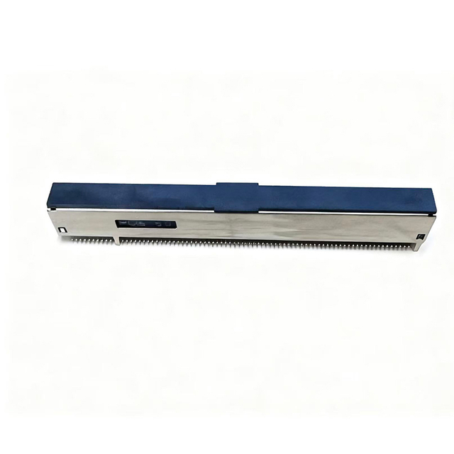
A connector must survive its intended operating environment. Standard consumer motherboards might only require 50 to 100 mating cycles. In contrast, industrial testing environments or server test benches demand robust contacts rated for 10,000+ cycles. Gold plating thickness on the contact pins directly correlates to the mating cycle lifespan.
Retention force and shock/vibration resistance matter immensely for CEM slots holding heavy GPUs. Ensure the chosen slot includes locking mechanisms or supports external retention clips. Additionally, verify thermal constraints. High-temperature plastics are necessary to survive reflow soldering profiles and withstand the continuous operating temperature ranges found in dense, poorly ventilated server chassis. Warpage during the reflow process can cause open circuits on SMT pins.
Always select components that have passed official PCI-SIG compliance workshops. Datasheets claiming a connector is "Gen 5 compatible" without official certification carry immense risk. Using non-certified connectors in enterprise hardware often leads to intermittent link training failures and field returns. Request the compliance test reports from the manufacturer before adding the part to your BOM. The PCI-SIG integrators list is the definitive source for verifying component compliance.
Translating connector selection into a functional, compliant board design requires strict adherence to high-speed routing principles. The breakout region underneath the connector is where most signal integrity issues originate. A poorly designed breakout will ruin the performance of even the most expensive connector.
Maintain consistent trace width and spacing to avoid impedance discontinuities at the connector breakout region. Necking down traces to fit between connector pins alters the impedance profile. Keep these transitions as short as physically possible. Use a 2D or 3D field solver to calculate the exact trace geometries required for your specific dielectric material and copper weight.
Adhere to standard board design guidelines by routing the differential clock lines using the identical trace geometries, widths, and spacing as the data differential pairs. This ensures uniform channel characteristics across the entire bus. Avoid sharp right angles in your routing; utilize smooth arcs or 45-degree chamfers to prevent signal reflection at corner junctions. Ensure that the P and N traces of a differential pair are routed symmetrically.
Treat vias as vertical interconnects that function as lumped parasitic elements. They introduce both capacitive and inductive penalties, which directly degrade channel impedance. In Gen 5 and Gen 6 designs, via optimization is mandatory. You cannot simply drop a standard via into a 32 GT/s channel and expect it to work.
Implement back-drilling to remove unused via stubs that act as resonant antennas. Specify the maximum allowable stub length in your fabrication notes (typically less than 10 mils for Gen 5).
Optimize anti-pad sizes on reference planes to tune the via impedance back to the target 85Ω or 100Ω. Larger anti-pads increase impedance, while smaller anti-pads decrease it.
Place ground return vias immediately adjacent to signal vias to maintain continuous return paths and minimize loop inductance. The ratio of signal vias to ground vias should ideally be 1:1 or 1:2 for high-speed transitions.
Avoid routing high-speed signals across split planes. If a signal must cross a split, provide stitching capacitors immediately adjacent to the crossing point.
Manage both intra-pair skew (length differences within the same differential pair) and inter-pair skew (length differences between different data lanes). Intra-pair skew must be kept extremely tight (often under 5 mils) to prevent mode conversion from differential to common-mode noise. Common-mode noise radiates EMI and degrades the differential signal quality.
Length matching for differential clocks to data lines is generally not required in modern PCIe architectures. The receiver circuitry handles this alignment, provided the differential clock is delivered cleanly and with minimal jitter to each device and connector. Focus your routing efforts on intra-pair matching rather than forcing the clock to match the longest data lane. Over-constraining the layout with unnecessary length matching rules leads to convoluted routing and increased board layers.
Balancing engineering ideals with procurement realities determines the final component selection. You must weigh assembly methods and performance margins against project constraints. The goal is to achieve reliable performance without over-engineering the solution.
SMT provides the superior signal integrity required for Gen 5 and Gen 6 applications because it eliminates the parasitic via stubs inherent to through-hole pins. However, SMT offers lower mechanical strength. If the board will endure heavy vibration, you must design supplementary mechanical support, such as through-hole mounting tabs on the connector shield.
PTH offers robust mechanical retention, simplifying assembly for heavy add-in cards. Yet, it introduces significant signal degradation at speeds exceeding 16 GT/s. If you must use PTH for a Gen 4 or Gen 5 design, heavily optimize the via transitions and mandate back-drilling in your fabrication notes. The choice between SMT and PTH often dictates the entire manufacturing flow for the PCB assembly.
Specify the component that meets the requirement without excessive padding. The financial impact of specifying a premium Gen 6 SMT connector with heavy gold plating for a Gen 3 industrial control board is unjustifiable. It inflates the BOM without providing any functional benefit to the end user. Match the connector specifications to the actual system requirements.
Consider supply chain availability. Multi-sourcing standard CEM footprints ensures manufacturing continuity. Proprietary footprints lock you into a single vendor, increasing lead time risks during component shortages. Always verify that multiple manufacturers can supply a connector with the exact same footprint and electrical characteristics before committing to a design.
As data rates continue to increase with PCIe Gen 5, Gen 6, and future Gen 7 platforms, selecting the right PCIe connector is critical for maintaining signal integrity, ensuring long-term reliability, and maximizing system performance. By evaluating connector type, electrical performance, PCB layout requirements, mechanical durability, and compliance standards, engineers can build scalable, future-ready hardware platforms that support demanding AI, networking, and enterprise computing applications.
Working with an experienced connectivity solutions provider is equally important for ensuring product quality and long-term reliability. CONSHAREA provides a comprehensive portfolio of high-performance PCIe connectors and interconnect solutions for servers, storage systems, AI computing, and networking equipment. With advanced engineering, strict quality control, and professional technical support, we help customers optimize signal integrity, simplify hardware design, and accelerate next-generation product development.
Download supplier 3D models and S-parameter files for your shortlisted components to begin architectural planning.
Run pre-layout 3D electromagnetic (EM) simulations to verify the connector footprint and via transitions against your specific PCB stack-up.
Request physical samples to perform mechanical fit-testing with your intended chassis, heat sinks, and add-in cards.
Review the manufacturer's PCI-SIG compliance documentation and test reports before finalizing the BOM.
A: A standard CEM slot provides 1.1A per contact pin for power delivery. The total power delivery scales by slot size. A standard x16 slot can deliver up to 75W directly through the motherboard connector, utilizing the 12V and 3.3V power pins. For higher power demands, supplementary power cables are required.
A: Yes, they are both mechanically and electrically backward compatible. You can insert a Gen 4 card into a Gen 5 slot. The host system will auto-negotiate the link during the boot sequence and operate at the Gen 4 maximum speed of 16 GT/s without any hardware modifications.
A: Mitigate crosstalk by assigning alternating ground pins between high-speed differential pairs where possible. Optimize anti-pad dimensions on the internal planes, and ensure you maintain strict differential pair spacing immediately as the traces exit the connector pads. Avoid routing adjacent pairs in parallel for long distances.
A: A CEM connector is a vertical or right-angle card-edge slot used for large add-in cards like GPUs and network adapters. An M.2 connector is a low-profile, parallel-to-board interface designed for compact applications, primarily used for NVMe storage drives and wireless communication modules in laptops and dense servers.
A: No, length matching the clock to data lines is not strictly required in modern architectures. The receiver circuitry handles the alignment. However, intra-pair length matching within the clock pair itself is critical. The differential clock must be delivered cleanly and symmetrically to each device.