
Views: 0 Author: Site Editor Publish Time: 2026-08-31 Origin: Site


Rigid printed circuit board interconnects carry hidden penalties when deployed in high-vibration environments and automated assembly lines. Engineers frequently encounter tolerance stacking, mechanical stress, and severe assembly bottlenecks when attempting to mate multiple rigid components. As hardware scales into modular architectures, minor alignment errors compound during manufacturing. This physical mismatch directly transfers kinetic energy and thermal expansion forces into the rigid joints. The result is solder joint fatigue, contact failure, elevated scrap rates, and eventual field recalls.
Addressing these mechanical limitations requires a structural shift in how boards interface. A Floating Board to Board Connector serves as an engineered solution designed specifically to absorb X, Y, and Z-axis deviations. By integrating a spring-like mechanism within the connector housing, this architecture decouples mechanical stress from electrical continuity. It allows mating interfaces to shift independently of the soldered base, ensuring reliable automated production and long-term operational stability under dynamic physical loads.
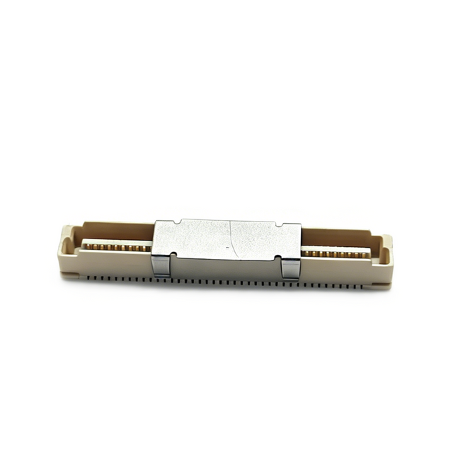
Misalignment Absorption: Floating mechanisms compensate for mating tolerances across multiple axes (typically up to ±1.0mm in X/Y and ±0.5mm in Z), ensuring secure connections even under dynamic conditions.
Stress Reduction: By absorbing kinetic energy and thermal expansion, these connectors drastically reduce the risk of solder cracks and PCB warping over the product lifecycle.
Manufacturing Efficiency: The self-aligning nature of floating connectors supports rapid, high-yield automated substrate assembly (pick-and-place) and blind mating scenarios.
Design Flexibility & Risk Reduction: Engineers can safely stack multiple boards or integrate modular subsystems without compounding rigid tolerance errors, significantly reducing development time and design risk.
Cable Elimination: Enables direct signal transfer between PCBs without the need for intermediary wiring, streamlining the Bill of Materials (BOM) and reducing manual assembly labor.
Table of Contents
Standard rigid electromechanical interconnects face severe physical limitations when subjected to external forces, thermal shock, or standard manufacturing variances. When two printed circuit boards are rigidly mated, any dimensional variation in the PCB substrate, the chassis, or the connector itself forces the assembly out of alignment. This misalignment places immediate shear and tensile stress on the surface mount technology (SMT) solder joints. Over time, thermal cycling and external vibration exacerbate this stress. The coefficient of thermal expansion (CTE) mismatch between the FR4 PCB material and the plastic connector housing causes the components to expand and contract at different rates. This constant microscopic movement leads to fractures in the solder and eventual open circuits.
The structural design of a floating connector mitigates this by utilizing a dual-body construction. The architecture consists of a stationary base soldered directly to the PCB and a movable receptacle or plug. These two segments are linked by a springform bed or a highly engineered spring-like terminal design. This internal geometry allows the mating interface to move independently of the fixed base while maintaining continuous, uninterrupted electrical contact. The spring terminals flex to absorb kinetic energy, effectively isolating the fragile solder tails from mechanical shock.
This internal flexibility provides X, Y, and Z-axis compensation. During the mating process, the connector geometry absorbs lateral shifts (the X and Y axes) and vertical deviations (the Z axis). If a robotic arm places a board slightly off-center, the floating receptacle shifts to guide the plug into place, preventing the plastic housings from binding or shattering. During continuous operation, this multi-axis float absorbs chassis flex and thermal expansion, ensuring the contact pins do not fret or wear prematurely. The terminals are typically formed into a U-shape or S-shape, providing the necessary elastic deformation required to sustain thousands of hours of vibration without yielding.
Selecting the appropriate interconnect requires understanding the baseline differences between available technologies. Rigid connectors suffice in static, single-board environments where tolerances are tightly controlled and no external vibration is present. Wire-to-board assemblies are traditionally used when boards are spaced far apart or positioned at irregular angles, though they introduce manual routing labor and signal degradation risks. Floating architectures become a strict engineering requirement when designers need to save space, eliminate manual wiring, and guarantee reliability in multi-board stacks subjected to dynamic environments.
Interconnect Technology Comparison
Feature | Rigid Connectors | Wire-to-Board Cables | Floating Connectors |
|---|---|---|---|
Mechanical Stress Absorption | None. Transfers stress directly to PCB solder joints. | High. Cables flex freely to absorb movement. | High. Internal spring terminals absorb X, Y, and Z deviations. |
Assembly Automation | Requires high-precision alignment. Prone to binding. | Manual assembly required. High labor dependency. | Excellent. Self-aligning design supports rapid pick-and-place. |
Space Efficiency (Z-Height) | Very high. Low-profile options readily available. | Low. Requires vertical clearance for cable routing and bend radius. | Moderate. Requires specific stacking heights for the spring mechanism. |
Signal Integrity at High Speeds | Excellent. Short signal paths minimize loss. | Variable. Long cables introduce crosstalk and insertion loss. | High. Engineered terminals maintain impedance control despite movement. |
In complex hardware assemblies, engineers often need to route signals between parallel boards using multiple connector pairs. With rigid connectors, the dimensional tolerances of each component stack on top of one another. Consider a scenario where the PCB fabrication has a ±0.1mm tolerance, the connector placement has a ±0.1mm tolerance, and the chassis mounting holes have a ±0.2mm tolerance. The total tolerance stack can easily reach 0.4mm. A rigid connector with only 0.1mm of clearance will bind, forcing the assembly technician to bend the board to make the connection. Floating connectors reset this tolerance baseline. The internal float allowance of each connector absorbs the local variance, allowing multiple connector pairs to be used on the same PCB without mechanical interference or forced alignment.
The physics of stress distribution dictate that mechanical energy will exploit the weakest point in an assembly. In traditional rigid setups, the SMT solder tails bear the brunt of mating impact, continuous vibration, and thermal cycling. The floating mechanism fundamentally alters this load path. By isolating the solder joints from the mating interface, the spring terminals absorb the kinetic energy. This isolation prevents the transmission of shear forces to the PCB pads, virtually eliminating the risk of pad cratering and solder cracks. Furthermore, it prevents the micro-fretting that degrades contact plating over time. Fretting corrosion occurs when microscopic movements wear away the gold plating, exposing the underlying nickel or copper to oxidation. The floating mechanism absorbs this movement, keeping the mating surfaces stable.
Modern manufacturing relies heavily on rapid robotic assembly to maintain throughput. Standard pick-and-place machines and robotic arms operate within specific tolerance windows. Vision systems align components based on fiducial markers, but substrate warpage or slight chassis variations cause local deviations. If a rigid connector is slightly misaligned during automated mating, the machine will either crush the connector or trigger an assembly fault, stopping the line. The self-aligning nature of a floating connector acts as a mechanical funnel. It guides the mating halves together despite minor positional errors. This lowers cycle times, improves overall production yield, and enables true blind mating scenarios where optical alignment is impossible.
Adopting a modular design strategy relies heavily on dependable interconnects. When engineering teams utilize floating interconnects, they gain the flexibility to swap, upgrade, or replace specific modular subsystems without redesigning the entire PCB architecture. If a sensor module requires a mid-cycle update, the existing floating interface accommodates the new board seamlessly, absorbing any slight dimensional changes in the new hardware. This decoupling of mechanical and electrical constraints reduces development time and minimizes design risk during iterative prototyping. Engineering teams spend less time troubleshooting mechanical interference and more time optimizing system performance.
Replacing bulky cable assemblies with direct board connections streamlines the entire operational footprint of a device. Manual cable routing is notoriously prone to human error. Technicians can pinch wires under chassis lids, seat connectors improperly, or route cables inconsistently, leading to unpredictable electromagnetic interference (EMI) profiles. A Floating Board to Board Connector eliminates these variables. By transferring signals directly between substrates, engineers reduce the overall device weight, shrink the required chassis volume, and remove the labor dependency associated with manual cable harness installation. The electrical path becomes shorter, more predictable, and entirely automated during assembly.
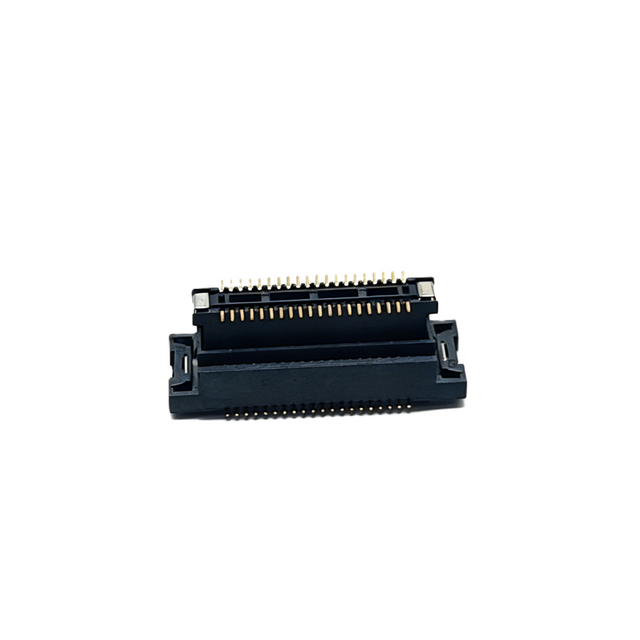
The automotive sector presents one of the most hostile environments for sensitive electronics. Advanced Driver Assistance Systems (ADAS), LiDAR modules, and central infotainment units are subjected to continuous engine vibration, road shock, and extreme thermal cycling. Standard rigid connectors fail rapidly under these conditions due to solder fatigue. Automotive engineering standards, such as ISO 16750, dictate rigorous vibration and mechanical shock profiles that components must survive. Floating interconnects are heavily specified in automotive hardware because they maintain electrical continuity while absorbing the constant kinetic energy of the vehicle. They meet strict automotive reliability standards and prevent catastrophic safety system failures by ensuring sensor data reaches the main processing unit without interruption.
Industrial environments demand hardware that can survive continuous mechanical stress while supporting modular maintenance. Motor controllers, Programmable Logic Controllers (PLCs), and robotic joint assemblies require rapid assembly and high reliability. In a robotic arm, the internal control boards experience high-frequency vibration and rapid acceleration during operation. Heavy machinery on the factory floor generates low-frequency, high-amplitude vibrations that transfer through equipment racks. Floating connectors allow internal PCBs to remain securely connected without transferring mechanical shock to delicate surface mount components. This ensures maximum uptime on the factory floor and allows maintenance technicians to quickly swap out faulty modules without wrestling with complex cable harnesses.
Server racks and high-capacity network switches operate in dense, space-constrained environments where modular upgrades are standard practice. Technicians frequently perform blind mating when sliding blade servers into backplanes or attaching expansion cards. Floating interconnects facilitate this blind mating by capturing the plug and guiding it into the receptacle despite the lack of visual feedback. The elimination of internal cable routing maximizes airflow within the chassis. Unobstructed airflow is a strict requirement for thermal management in high-density data centers, where overheating leads to processor throttling and reduced network throughput.
Industry Application Requirements
Industry | Primary Environmental Challenge | Floating Connector Benefit |
|---|---|---|
Automotive (ADAS, LiDAR) | Continuous road vibration and extreme thermal cycling (-40°C to +125°C). | Absorbs kinetic energy, preventing solder joint fatigue and contact fretting. |
Industrial Automation | High-frequency machine vibration and rapid robotic acceleration. | Isolates SMT pads from mechanical shock, ensuring continuous sensor data flow. |
Telecommunications | Dense packaging, blind mating requirements, and thermal management. | Enables cable-free blind mating, improving chassis airflow and modularity. |
Specifying the correct connector requires balancing the demand for miniaturization with the physical realities of mechanical float. As pitch sizes decrease to 0.5mm or 0.4mm to accommodate high pin counts in compact devices, the internal space available for the springform bed also shrinks. Engineers must verify that the chosen micro-pitch connector still provides adequate X and Y-axis compensation. A 0.5mm pitch connector typically offers ±0.5mm of float, whereas a larger 0.8mm pitch connector might offer up to ±1.0mm. Designers must ensure the selected pitch provides enough float to cover the calculated tolerance stack of the specific assembly without compromising the structural integrity of the housing or the normal force of the contacts.
When routing high-speed protocols such as PCIe, USB 3.0, or Gigabit Ethernet, the mechanical design of the interconnect directly impacts signal integrity. The spring-like terminals in a floating connector can introduce impedance mismatches or act as small antennas if not properly designed. The length and shape of the spring terminal add parasitic inductance and capacitance to the signal path. Evaluating these connectors requires strict scrutiny of insertion loss, return loss, and crosstalk metrics. High-speed variants incorporate specialized ground planes, optimized terminal geometries, and specific dielectric materials to maintain strict 85-ohm or 100-ohm impedance control across the floating interface.
Routing power alongside data requires careful thermal management. Standard signal contacts may only support 0.5A per pin, which is insufficient for main power distribution. Pushing too much current through a small spring terminal causes excessive resistive heating, which can melt the plastic housing or relax the spring tension. Engineers must decide between using dedicated power floating connectors or power-signal hybrid connectors. Hybrid designs incorporate larger, heavier-gauge copper terminals at the outer edges of the housing to handle higher currents (e.g., 3A to 5A per pin). This isolates the thermal rise from the sensitive high-speed signal pins located in the center of the array, keeping the overall temperature rise within safe operational limits.
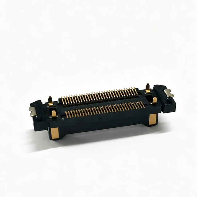
The operating environment dictates the required material specifications. For high-temperature applications or environments with corrosive outgassing, the housing plastics must be molded from Liquid Crystal Polymer (LCP) or similar high-temp resins capable of withstanding reflow profiles and operational heat. The contact plating is equally important for longevity. Gold over nickel plating is standard for ensuring low contact resistance and preventing oxidation. The thickness of the gold plating (e.g., 15 microinches vs. 30 microinches) determines the connector's durability rating. Applications requiring a high number of mating cycles during testing or modular field replacements demand thicker plating to withstand repeated mechanical wear.
Connector Evaluation Matrix
Evaluation Criteria | Primary Engineering Consideration | Impact on Hardware Design |
|---|---|---|
Pitch & Pin Count | Balancing miniaturization with required float allowance. | Determines PCB footprint and maximum trace density. |
Signal Integrity | Impedance control, insertion loss, and crosstalk limits. | Dictates compatibility with high-speed protocols (PCIe, Ethernet). |
Current Rating | Thermal rise and contact normal force under load. | Drives the choice between hybrid power/signal or dedicated power connectors. |
Durability & Plating | Gold over nickel thickness and LCP housing materials. | Ensures reliability across specified mating cycles and thermal extremes. |
Integrating floating mechanisms introduces a higher initial unit complexity compared to standard rigid alternatives due to the dual-body molding and specialized spring terminals. Procurement and engineering teams must weigh this upfront specification against long-term lifecycle reliability. The reduction in warranty claims caused by vibration-induced failures, the decrease in assembly line defect rates, and the complete elimination of manual cable harness labor typically yield a net positive outcome for high-reliability hardware. By preventing field failures related to solder joint fatigue, manufacturers protect their brand reputation and reduce the logistical burden of processing returns and repairs.
The mechanical reality of a floating architecture requires physical space to operate. The dual-housing design and internal spring bed inherently demand a larger PCB footprint and specific stacking heights compared to standard low-profile rigid connectors. Designers must account for this space penalty early in the layout phase. They must ensure that the necessary keep-out zones are respected on the PCB to prevent adjacent components from interfering with the floating housing's movement. Furthermore, the mechanical engineering team must verify that the chassis provides adequate Z-height clearance for the specified mating distance, ensuring the boards can be fully seated without bottoming out the connector.
In environments subjected to specific, sustained vibration frequencies, the internal spring terminals can theoretically experience mechanical resonance. If the external vibration matches the natural frequency of the spring terminal, it amplifies the motion, leading to momentary contact separation or accelerated fretting wear. Thorough vibration profiling is required to ensure the connector's natural frequency does not overlap with the operating environment. The exposed gap between the floating and fixed housings can create EMI shielding vulnerabilities. In noisy RF environments, engineers must specify shielded floating connectors that incorporate a continuous metal shell to maintain EMC compliance and prevent signal degradation.
Successful implementation relies on proactive design strategies. Utilizing guide pins on the PCB or chassis helps pre-align the boards before the connectors engage, reducing the initial mating stress and preventing severe angular misalignment. Optimizing the PCB layout to provide structural support near the connector base prevents board flex during insertion. Placing mounting screws close to the connector anchors the substrate, forcing the floating mechanism to do the work rather than the FR4 board. Conducting thorough vibration and thermal shock testing during the early prototyping phase ensures the selected float allowance adequately covers the real-world mechanical deviations of the final assembly.
Review manufacturer datasheets to confirm the exact X, Y, and Z-axis float allowances for your required pitch size.
Request 3D CAD models to run mechanical tolerance simulations and verify chassis clearances.
Order physical samples to conduct prototype mating tests and validate automated pick-and-place compatibility.
Perform environmental vibration testing on early prototypes to confirm solder joint integrity under load.
For projects that require reliable and application-specific interconnection solutions, CONSHARE focuses on precision connector development and manufacturing, supporting customers from connector selection and design evaluation to customization and volume production. With engineering and manufacturing capabilities covering a wide range of connector applications, CONSHARE helps customers develop dependable interconnection solutions for automotive electronics, industrial equipment, communications hardware, and other demanding electronic systems.
A: Most standard floating connectors can absorb up to ±1.0mm of misalignment in the X and Y axes, and approximately ±0.5mm in the Z axis. Exact tolerances depend on the specific pitch size and manufacturer design. Micro-pitch variants offer slightly less mechanical travel due to space constraints.
A: They utilize a dual-body design with internal spring terminals. When boards experience vibration or thermal expansion, the spring mechanism flexes and absorbs the kinetic energy. This isolates the surface mount solder tails from mechanical stress, preventing the shear forces that cause cracking.
A: Yes. Many modern floating connectors are engineered for high-speed protocols like PCIe Gen 4, USB 3.2, and Gigabit Ethernet. They utilize optimized terminal geometries and impedance-controlled designs to minimize insertion loss and crosstalk despite the moving mechanical parts.
A: A floating connector features internal moving parts to absorb dimensional tolerances and vibration. A blind mating connector features exaggerated guide ramps and funnels to help align components without visual assistance. Many floating connectors incorporate blind mating features, but not all blind mating connectors float.
A: Floating connectors eliminate the need for physical cables, reducing device weight, freeing up chassis space, and removing the manual labor and error risks associated with routing wires. They provide a direct, rigid-yet-flexible connection between substrates, whereas cables are used for long-distance routing.
A: Yes. Hybrid floating connectors integrate dedicated, heavy-gauge power terminals alongside standard signal pins. This allows a single connector to safely route higher currents (often 3A to 5A per power pin) while simultaneously handling sensitive data streams, saving valuable PCB space.
A: Automated pick-and-place machines operate with slight positional variances. A rigid connector might bind or crush if misaligned during robotic mating. The self-aligning nature of a floating connector absorbs these minor robotic placement errors, preventing line stoppages, reducing scrap, and increasing overall manufacturing yield.


