
Views: 0 Author: Site Editor Publish Time: 2026-08-31 Origin: Site


The transition to DDR5 architecture doubles data rates and bandwidth compared to DDR4, but this performance leap introduces severe signal integrity (SI), thermal, and mechanical challenges directly at the motherboard interface. Specifying an inadequate memory socket leads to impedance mismatches, high crosstalk, failed JEDEC compliance, and ultimately, costly PCB respins or field failures in high-performance computing environments. To mitigate manufacturing risks and ensure system reliability, hardware architects must evaluate a DDR5 Connector based on strict mechanical tolerances, mounting technologies, environmental durability, and empirical signal integrity data. You cannot treat this interface as a simple mechanical bridge; it acts as a highly sensitive RF transmission line. This guide details the technical criteria for shortlisting and integrating these components, focusing on physical layout constraints, power delivery shifts, and the exact manufacturing tolerances required to maintain high-speed data integrity across your hardware platforms.
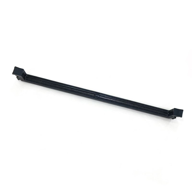
Form Factor Incompatibility: DDR5 connectors feature unique keying and pin counts (e.g., 288-pin for standard DIMM, 262-pin for SO-DIMM) preventing backward compatibility with DDR4 modules.
Signal Integrity Dictates Mounting: Surface Mount Technology (SMT) is overwhelmingly required for DDR5 over Plated Through-Hole (PTH) to minimize stub lengths and support 4.8 to 8.4 Gbps+ data rates.
Power Architecture Shift: The relocation of the Power Management IC (PMIC) directly onto the memory module changes the power delivery requirements, grounding distribution, and thermal profile at the connector interface.
Manufacturing Yield Risks: High-density SMT connectors require precise coplanarity controls (≤ 0.10mm) and high-temperature thermoplastic housings to prevent solder joint failure and PCB warpage during reflow.
Table of Contents
Integrating modern memory architectures demands a complete overhaul of your hardware design approach. The socket operates as a high-speed transmission component within the RF pathway. Any physical imperfection in the contact interface translates directly into electrical degradation. Engineers must treat the memory socket with the same rigorous signal integrity analysis applied to PCIe Gen 5 or 400G Ethernet interfaces. Failure to account for parasitic capacitance or inductance at the socket level closes the data eye, resulting in unacceptable bit error rates. We see layout teams frequently underestimate the impact of the connector body on the overall channel loss budget, leading to failed validation testing late in the development cycle.
DDR5 establishes a massive leap in throughput. Initial specifications target 4.8 Gbps, with the standard scaling rapidly toward 8.4 Gbps. At these frequencies, the Nyquist frequency reaches 4.2 GHz. Wavelengths become short enough that the physical dimensions of the connector pins act as antennas. This drastically reduces the available margin for insertion loss, return loss, and jitter. The electrical length of the contact pin must be precisely controlled. Even a fraction of a millimeter in excess stub length creates destructive resonance. Hardware teams must scrutinize the insertion loss profiles provided by connector manufacturers, ensuring they meet the strict limits defined by JEDEC across the entire frequency band. You need to verify that the contact geometry minimizes impedance discontinuities as the signal transitions from the motherboard pad, through the pin, and into the module edge finger.
Frequency vs. Insertion Loss Targets
Data Rate (Gbps) | Nyquist Frequency (GHz) | Max Allowable Insertion Loss (dB) | Target Return Loss (dB) |
|---|---|---|---|
4.8 | 2.4 | -0.5 | -15 |
5.6 | 2.8 | -0.6 | -14 |
6.4 | 3.2 | -0.7 | -12 |
8.4 | 4.2 | -0.9 | -10 |
Physical constraints heavily influence component selection. Standard DIMM sockets utilize a dense 0.85mm pitch, while SO-DIMM variants compress this further to a 0.50mm pitch. This extreme density leaves zero tolerance for mechanical misalignment. Precision manufacturing is mandatory. If the plastic housing warps by even a few microns, the contact pins will not align perfectly with the module pads. This misalignment changes the wiping distance, altering the contact resistance and degrading the signal. Furthermore, the tight pitch forces PCB designers to use ultra-fine trace routing and microvias to escape the connector footprint without violating clearance rules. You must coordinate closely with your bare board fabricator to ensure they can reliably etch the required trace widths and spaces between the surface mount pads.
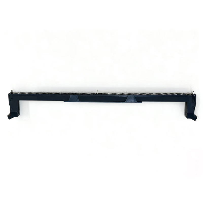
Procurement and engineering teams must align the physical form factor with the intended operating environment. Each category adheres to specific JEDEC standards dictating mechanical outlines, pin counts, and electrical baselines. Selecting the correct variant depends entirely on the chassis constraints, thermal strategy, and target application. You cannot simply swap one form factor for another without redesigning the entire memory subsystem layout.
Enterprise servers, high-end workstations, and desktop PCs rely on standard DIMM form factors. These utilize a 288-pin vertical orientation compliant with the JEDEC MO-329 specification. While the physical socket remains identical across Unbuffered (UDIMM), Registered (RDIMM), and Load-Reduced (LRDIMM) modules, the thermal loads vary significantly. RDIMMs and LRDIMMs generate more heat, requiring robust connector housings capable of withstanding sustained high temperatures without deforming.
Latching mechanisms require careful evaluation. Manufacturers offer standard, narrow, and ultra-narrow ejectors. Standard ejectors provide excellent leverage for module extraction but consume valuable lateral board space. Ultra-narrow ejectors allow designers to pack memory channels closer together. This density proves necessary in 1U or 2U server chassis where airflow routing and component proximity dictate system performance. When specifying ultra-narrow ejectors, verify that your assembly technicians can still actuate the latches without specialized tools.
Laptops, micro-PCs, and edge computing devices utilize Small Outline DIMM (SO-DIMM) sockets. These 262-pin connectors comply with the JEDEC MO-337 standard. They are available in both right-angle and vertical orientations. Right-angle versions lay the memory module parallel to the motherboard, minimizing the z-axis height. This orientation dominates mobile and embedded designs where vertical space is severely restricted.
Profile height is the primary selection variable for right-angle SO-DIMMs. Standard heights include 4.0mm, 5.2mm, and 8.0mm. A 4.0mm profile offers the thinnest possible device footprint but restricts the placement of other components underneath the socket. An 8.0mm profile provides enough clearance to route traces or place low-profile capacitors directly beneath the memory module, optimizing overall board utilization. You must balance the need for a thin device profile against the routing density requirements of the motherboard.
The Compression Attached Memory Module (CAMM2) standard represents a low-profile, high-signal-integrity alternative to traditional SO-DIMMs. Instead of an edge-card insertion mechanism, CAMM2 uses a compression interface. This eliminates the traditional pin-and-socket mating, drastically reducing the signal path length. It proves highly advantageous for ultra-thin mobile workstations requiring massive capacity and pristine signal integrity. However, CAMM2 requires specific mounting hardware and backplates to ensure even compression force across the entire contact array, adding mechanical complexity to the system assembly.
DDR5 Form Factor Comparison
Form Factor | Pin Count | Pitch | JEDEC Standard | Typical Application |
|---|---|---|---|---|
Standard DIMM | 288-pin | 0.85mm | MO-329 | Servers, Desktops, Workstations |
SO-DIMM | 262-pin | 0.50mm | MO-337 | Laptops, Mini-PCs, Edge Devices |
CAMM2 | Varies | Compression | JESD318 | Ultra-thin Workstations |
Evaluating supplier datasheets requires translating physical specifications into electrical and mechanical outcomes. Hardware engineers must look past basic pin counts and scrutinize the materials, plating, and mounting technologies that define long-term reliability. A datasheet might list compliance with a standard, but you need to dig into the test conditions to ensure they match your actual deployment environment.
Surface Mount Technology (SMT) is the undisputed industry standard for DDR5 integration. SMT eliminates the plated through-hole via stubs inherent in PTH designs. At 4.8 Gbps and above, a via stub acts as an open-ended transmission line, reflecting signals and causing deep resonant nulls in the frequency response. SMT pads keep the signal on the surface layer, allowing for immediate transition into microstrip routing or controlled via transitions to internal stripline layers. We strongly advise against using any through-hole components in the high-speed memory path.
Press-Fit technology maintains a niche presence in exceptionally thick server backplanes where SMT reflow is physically impossible due to thermal mass. However, Press-Fit introduces severe signal integrity trade-offs. The compliant pin requires a large via barrel, creating massive parasitic capacitance. Engineers using Press-Fit must employ aggressive back-drilling techniques to remove the unused via stub, adding significant cost and complexity to the bare board fabrication process. If you must use Press-Fit, mandate strict back-drill depth tolerances from your PCB manufacturer.
Maintaining a strict 85-ohm differential impedance through the connector is non-negotiable. Impedance discontinuities cause signal reflections, degrading the return loss. You must review the Time Domain Reflectometry (TDR) plots provided by the connector manufacturer to verify impedance stability across the entire contact length. Look for a flat TDR profile without sharp dips or spikes.
Crosstalk mitigation relies heavily on optimized contact geometries. Near-End Crosstalk (NEXT) and Far-End Crosstalk (FEXT) occur when electromagnetic fields couple between adjacent pins. High-quality DDR5 Connector designs utilize specific pin shapes and optimized plastic dielectrics to isolate signals. The distribution of ground pins among the signal pairs provides immediate return paths and shields against aggressive coupling. You should request the full S-parameter matrix from the vendor to simulate the exact crosstalk levels in your specific layout.
Contact plating dictates the lifespan and reliability of the mating interface. The industry standard is typically 15µin of gold plating over a nickel underplate. This configuration provides adequate protection against oxidation and supports roughly 25 mating cycles, which is sufficient for standard consumer and enterprise hardware where modules are rarely swapped.
Industrial, automotive, or test-fixture applications demand 30µin of gold plating. Thicker gold resists fretting corrosion caused by micro-vibrations over time. When a system vibrates, the module shifts microscopically within the socket. This movement wears away thin plating, exposing the base metal to oxidation and drastically increasing contact resistance. Specifying 30µin gold mitigates this failure mode entirely. We also recommend inspecting the normal force specifications; the contact must maintain at least 30 grams of force against the module pad to ensure a gas-tight seal.
Systems deployed outside climate-controlled data centers face harsh environmental realities. Industrial edge devices and ruggedized telecom equipment require connectors with enhanced shock and vibration resistance. Look for specifications detailing performance under MIL-STD or specific IEC vibration profiles. The latching mechanism must maintain adequate normal force against the module pads even under continuous mechanical stress. If the latches fail, the module will unseat, causing an immediate system crash.
Environmental compliance is equally critical. Specify UL94V-0 flammability ratings to ensure the plastic housing self-extinguishes in the event of a thermal runaway. Halogen-free housing materials are mandatory to meet global environmental regulations, including RoHS and REACH, ensuring the product can be legally sold and deployed in international markets. Do not accept components without verifiable compliance certificates.
The DDR5 architecture introduces systemic changes that directly alter the operating environment of the socket. The most significant architectural shift is the relocation of power management components. This changes how you route power on the motherboard and how the connector handles thermal dissipation.
Previous memory generations relied on the motherboard to step down voltage and deliver clean power to the DIMM. DDR5 moves the Power Management IC (PMIC) directly onto the memory module. The motherboard now supplies a bulk 12V (or 5V) feed to the socket. The connector's power pins must handle higher current ratings to support this localized power conversion. You must ensure the power pins are rated for at least 1.0A to 1.5A per pin to handle the inrush current during system boot.
This shift demands an optimized ground pin distribution. The Power Delivery Network (PDN) requires low-inductance return paths to function efficiently. If the grounding scheme through the connector is inadequate, the PMIC will struggle with voltage droop during transient load spikes. Engineers must verify that the connector's current carrying capacity per pin aligns with the maximum theoretical draw of fully populated, high-capacity modules. Simulate the PDN impedance from the motherboard VRM, through the connector, to the PMIC input capacitors.
Placing the PMIC on the module generates localized heat directly above the socket interface. This thermal load transfers down the module contacts and into the connector housing. Continuous operation in dense server chassis pushes ambient temperatures near the socket well above 85°C. You must account for this heat when selecting the connector material.
Connector housings must be molded from High-Temperature Thermoplastics, such as Liquid Crystal Polymer (LCP). LCP maintains extreme dimensional stability under heat. It prevents the housing from warping during the 260°C peak temperatures of the IR reflow soldering process. Post-manufacturing, LCP ensures the socket does not deform under continuous operational heat, which would otherwise compromise the normal force of the contact pins and lead to intermittent electrical failures. Avoid older nylon-based plastics like PA46, as they absorb moisture and blister during lead-free reflow.
Selecting a high-performance socket is only half the battle. Poor PCB layout and flawed manufacturing processes will instantly negate the electrical benefits of a premium component. Hardware teams must enforce strict design and assembly guidelines to ensure the physical board matches the simulated performance.
Breakout routing beneath the connector footprint requires meticulous planning. Designers must use via-in-pad plated over (VIPPO) technology or precise dog-bone breakouts to transition signals to internal layers without violating the 0.85mm or 0.50mm pitch constraints. Trace length matching must account for the physical propagation delay inside the connector itself. The electrical length of a pin near the edge of the socket may differ slightly from a pin near the center. You must input the connector's specific pin delay values into your EDA tool to ensure accurate intra-pair and inter-pair skew matching.
Maintain continuous reference planes beneath the connector footprint. Voids in the ground plane directly under the surface mount pads create sudden impedance spikes. Route high-speed signals on stripline layers sandwiched between solid ground planes to contain electromagnetic fields and prevent crosstalk with adjacent memory channels.
Assign specific pin delay values in your EDA tool before starting the length matching process.
Route all high-speed memory signals on internal stripline layers to minimize EMI and crosstalk.
Ensure solid, uninterrupted ground reference planes exist directly above and below the routing layers.
Use VIPPO for all ground and power pins to reduce inductance and save routing space on the surface layer.
Maintain at least a 3W spacing rule between adjacent memory channels to prevent inter-channel crosstalk.
High-density SMT connectors are notoriously difficult to solder reliably. The primary manufacturing risk is poor coplanarity. Coplanarity measures the maximum vertical deviation among all the SMT leads on the bottom of the connector. For DDR5, coplanarity must strictly be ≤ 0.10mm. We reject any batches that exceed this tolerance.
If one pin sits 0.15mm higher than the rest, it will not make contact with the printed solder paste during placement. During reflow, this results in an open solder joint. Conversely, excessive solder paste applied to compensate for bad coplanarity leads to solder bridging and short circuits between the tightly pitched pins. Recommend automated optical inspection (AOI) and 3D X-ray inspection protocols for all memory socket solder joints to catch these defects before functional testing. Work with your contract manufacturer to optimize the solder stencil thickness and aperture design specifically for the memory socket footprint.
Pre-layout simulation is mandatory. Do not rely on generic rules of thumb. You must obtain accurate S-parameter models (Touchstone files) and 3D step files from the supplier. Import these models into 3D full-wave electromagnetic field solvers like Ansys HFSS or Keysight ADS. Simulate the entire channel—from the CPU die, through the motherboard routing, through the connector model, and into the memory module. This validates that the insertion loss and crosstalk remain within JEDEC specifications before committing to a costly PCB fabrication spin. Run eye diagram simulations at the target data rate to verify sufficient voltage and timing margins.
Supply chain volatility remains a constant threat to production schedules. Avoid designing a motherboard around a proprietary connector footprint. Select components that utilize standardized PCB land patterns. This allows procurement teams to dual-source the socket from multiple vendors without requiring a board redesign if the primary supplier faces lead-time disruptions. Verify that the alternative supplier's part matches both the mechanical footprint and the electrical performance baseline. Test samples from all approved vendors on your prototype boards to ensure they perform identically under load.
A DDR5 memory socket operates as a highly tuned RF component. The leap to 4.8 Gbps and beyond leaves no room for physical imperfections or poor material choices. Selecting a low-cost, unverified connector introduces unacceptable risks to system stability, JEDEC compliance, and data integrity. Impedance mismatches and crosstalk will inevitably lead to random system crashes under heavy memory loads. You must treat the selection and integration of this component with the highest level of engineering rigor.
Prioritize SMT mounting to preserve signal integrity and eliminate via stubs. Select profile heights and ejector styles based strictly on your chassis dimensions and thermal airflow requirements. Mandate strict coplanarity limits (≤ 0.10mm) and demand empirical SI data to ensure high manufacturing yields and reliable field performance. Do not compromise on contact plating thickness if your system will deploy in harsh environments.
For projects that require dependable high-speed interconnect performance, CONSHARE brings 20 years of experience in precision connector technology, integrating design, development, production, and sales to support diverse connector requirements. With established manufacturing capabilities and experience across PCB, USB, PCIe, power, and SAS connector solutions, CONSHARE provides a strong foundation for customized connectivity needs in data centers, consumer electronics, industrial automation, and automotive applications.
Request full S-parameter models and SI simulation reports from your shortlisted suppliers to validate channel performance in your EDA tools.
Download 3D CAD models to verify mechanical clearances, ejector sweep paths, and thermal airflow routing in your chassis design.
Order physical samples and build test boards to validate SMT reflow profiles and inspect solder joint reliability using 3D X-ray.
Verify environmental compliance certificates, including UL94V-0 and Halogen-free documentation, to ensure global market readiness.
A: The pin count depends on the form factor. Standard DIMM connectors, used in desktops and servers, feature 288 pins and comply with the JEDEC MO-329 specification. SO-DIMM connectors, designed for laptops and compact devices, feature 262 pins and comply with the JEDEC MO-337 specification.
A: No. DDR5 sockets feature unique mechanical keying. The alignment notch is positioned differently to physically prevent the insertion of DDR4 modules. This prevents electrical damage, as DDR5 operates at different voltages and utilizes a completely different pinout architecture.
A: SMT is preferred because it eliminates the plated through-hole via stubs found in PTH designs. At DDR5 frequencies (>4.8 Gbps), via stubs act as antennas, creating parasitic capacitance and destructive signal reflections. SMT keeps signals on the surface, ensuring clean, high-speed transmission.
A: JEDEC standards define the mechanical outlines, pin pitches, and mating forces. They also establish strict coplanarity limits (typically ≤ 0.10mm) for SMT leads and set electrical performance baselines, including maximum allowable insertion loss, return loss, and crosstalk parameters across specific frequency bands.
A: The PMIC shifts power management to the module, requiring the motherboard to supply a bulk 12V or 5V feed. The connector must handle higher current per power pin. Additionally, the PMIC generates localized heat, requiring the connector housing to be made from high-temperature thermoplastics to prevent warping.
A: The standard requirement for DDR5 routing is an 85-ohm differential impedance. Maintaining this specific impedance through the PCB traces and across the connector interface is critical to minimizing signal reflections and ensuring data integrity at high frequencies.
A: Yes. Industrial-grade variants feature thicker 30µin gold plating to resist fretting corrosion. They utilize enhanced latching mechanisms for superior shock and vibration resistance and are constructed with materials rated for extended temperature ranges, making them suitable for harsh edge computing environments.


