
Views: 0 Author: Site Editor Publish Time: 2026-08-31 Origin: Site


The transition to higher-speed memory architectures like DDR4 and DDR5 fundamentally shifts the margin for error in hardware design. The physical memory interface now acts as a primary bottleneck for system performance. Selecting a substandard or improperly specified memory socket leads to severe consequences. You risk signal degradation, impedance mismatches, and thermal throttling. Ultimately, these issues cause catastrophic system failure in high-availability environments like data centers and supercomputers. Engineering a reliable memory interface with a DDR Connector requires strict evaluation. You must analyze electrical tolerances, mechanical retention, and JEDEC standard compliance. This guide provides a technical framework for evaluating and selecting the optimal connector for your specific PCB architecture and application environment.
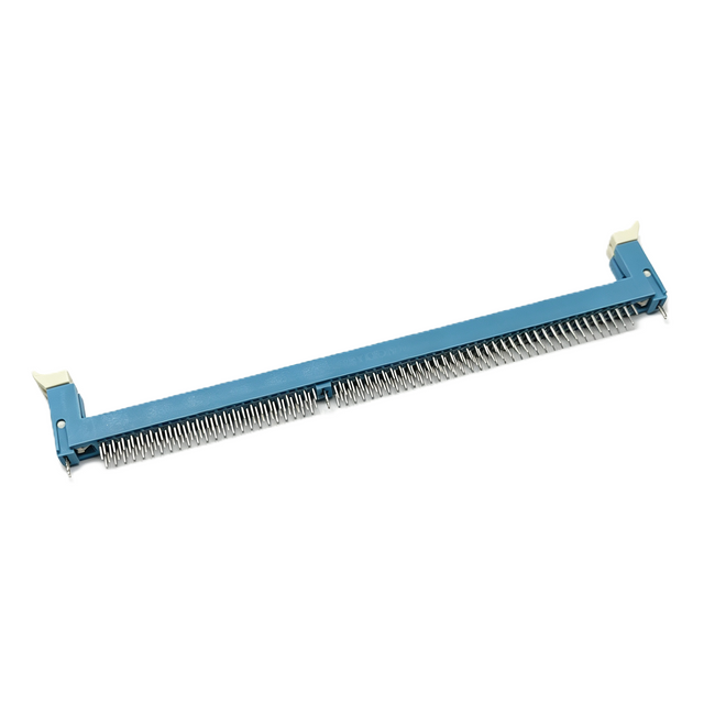
JEDEC Standard Compliance is Non-Negotiable: Ensure the selected connector strictly adheres to the mechanical and electrical specifications dictated by JEDEC for the specific DDR generation (DDR3, DDR4, or DDR5).
DDR5 Introduces New Power and Signal Demands: The shift of power management ICs (PMICs) to the memory module in DDR5 requires connectors with superior thermal dissipation and modified pin layouts compared to DDR4.
Mechanical Retention Dictates Reliability: For industrial or rugged applications, standard latching mechanisms are insufficient; evaluating mating cycles, vibration resistance, and shock tolerances is critical.
Signal Integrity Requires Holistic PCB Co-Design: A high-quality connector cannot compensate for poor PCB routing; insertion loss, crosstalk, and impedance must be evaluated as a combined connector-PCB system.
Table of Contents
A successful memory implementation provides a seamless electrical bridge. It connects the memory module directly to the motherboard. You need near-zero signal distortion at gigatransfer speeds. We define success on the bench by measuring the eye diagram opening at the receiver. A robust socket maintains signal integrity across all operating conditions. It ensures stable power delivery while minimizing electromagnetic interference. You must evaluate the physical interface as a high-frequency transmission line. Treat every pin as a critical component in the signal path.
Failing to specify the correct socket carries heavy operational penalties. Substandard contacts increase bit error rates (BER). High BER forces the system into constant error correction. This degrades overall computational throughput. Eventually, marginal connections cause complete system crashes. Field replacements for faulty motherboard components drain engineering resources and cause severe downtime. You cannot afford intermittent memory failures in mission-critical hardware.
Data transfer rates have evolved rapidly over the last decade. DDR3 operated comfortably at 2133 MT/s. Modern DDR5 architectures push speeds beyond 8400 MT/s. This massive increase compresses physical and electrical tolerances. High-speed signals suffer from skin effect and dielectric loss. Older socket designs cannot handle these modern frequencies. Manufacturers must tighten manufacturing tolerances. They use advanced plastics and optimized contact geometries to survive these speeds. The mechanical stress from heavy, modern heatsinks attached to memory modules also places unprecedented strain on the socket housing.
Engineers choose memory sockets based on form factor and application constraints. Each category serves a specific architectural need. You must match the physical footprint to your board's spatial limitations and thermal routing strategy.
Standard Dual In-Line Memory Module sockets represent the backbone of high-performance computing. They dominate environments where physical space allows for vertical module insertion.
Target applications include enterprise servers, supercomputers, desktop workstations, and data centers.
They feature a high pin count. DDR4 and DDR5 versions utilize 288 pins with a tight 0.85mm pitch.
The vertical orientation maximizes memory capacity support across the motherboard.
Engineers optimize these sockets for rack density and direct front-to-back airflow cooling.
They support registered (RDIMM) and load-reduced (LRDIMM) memory modules for massive RAM pools.
Small Outline DIMM sockets provide a compact alternative for mobile and embedded systems. They sacrifice maximum capacity for a significantly reduced physical footprint.
Target applications focus on laptops, compact industrial PCs, and edge computing devices.
They offer a significantly smaller footprint than standard DIMMs, typically utilizing 260 pins for DDR4 or 262 pins for DDR5.
Horizontal or angled mounting options save vertical space, allowing for ultra-thin chassis designs.
Designers use them primarily for space-constrained PCB layouts where vertical clearance is less than 10mm.
They utilize lateral retention clips rather than vertical ejector latches to secure the module.
These specialized sockets bridge the gap between standard DIMMs and SO-DIMMs. They offer high reliability in networking and telecommunications hardware.
Target applications span networking equipment, telecommunications routers, and embedded systems.
They provide specialized form factors balancing high density with reduced board space.
These sockets withstand harsh environments often found in outdoor telecom enclosures.
They support ECC (Error-Correcting Code) memory in compact footprints, ensuring data integrity in headless systems.
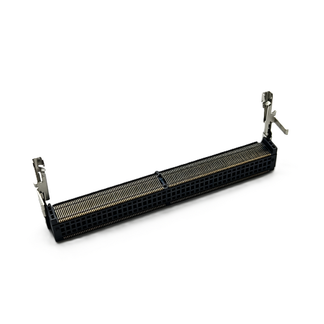
The push for thinner devices and higher bandwidth drives new socket architectures. These designs abandon traditional slotted insertion for direct compression or soldered alternatives.
Target applications include ultra-thin mobile devices, graphics processing, and high-performance computing.
They address the shift toward Compression-Attached Memory Modules (CAMM2).
CAMM2 achieves higher speeds without soldering modules directly to the board, utilizing a compression connector that mounts flat against the PCB.
Specialized testing sockets and interposers help engineers develop GDDR memory systems.
These designs minimize trace lengths to support extreme bandwidth requirements, often exceeding 10,000 MT/s.
Standard commercial sockets fail rapidly in extreme environments. Ruggedized variants incorporate mechanical and material upgrades to survive shock, vibration, and corrosive atmospheres.
Target applications cover aerospace, military, and heavy industrial environments.
They feature enhanced gold plating for superior corrosion resistance and extended mating cycles.
Specialized retention clips and screw-down brackets prevent module ejection during heavy vibration.
They offer compatibility with conformal coatings used to protect boards from moisture and dust.
Engineers specify high-temperature plastics to survive extreme thermal cycling in unconditioned environments.
Table 1: Memory Socket Form Factor Comparison
Form Factor | Typical Pin Count (DDR5) | Mounting Orientation | Primary Application | Retention Mechanism |
|---|---|---|---|---|
Standard DIMM | 288 Pins | Vertical | Servers, Desktops | End Ejector Latches |
SO-DIMM | 262 Pins | Horizontal / Angled | Laptops, Mini PCs | Lateral Spring Clips |
Mini-DIMM | 288 Pins | Vertical / Angled | Networking, Telecom | End Ejector Latches |
CAMM2 | Compression Array | Flat / Surface Mount | Ultra-thin Mobile | Screw-down Bracket |
DDR4 and DDR5 sockets look similar at a glance. Both utilize 288 pins for standard DIMM applications. However, mechanical keying differences prevent accidental insertion. The alignment notch on a DDR5 module sits closer to the center. You cannot force a DDR4 module into a DDR5 socket. This physical barrier protects the motherboard from incompatible voltage levels. Pin pitch remains tight at 0.85mm, demanding precise manufacturing. The internal contact design differs significantly to support higher frequencies. DDR5 contacts feature shorter electrical stubs and optimized geometries to reduce parasitic capacitance.
Power delivery architecture changed drastically between generations. DDR4 relies on the motherboard to regulate voltage. The motherboard supplies 1.2V directly to the memory pins. DDR5 shifts the power management IC (PMIC) directly onto the memory module. The motherboard now supplies 5V to the socket. The on-module PMIC steps this down to 1.1V. This reduces motherboard power routing complexity. However, it increases localized thermal stress at the connector level. The socket must handle higher current on specific 5V power pins without degrading the plastic housing or contact plating.
Signal integrity requirements define the true difference between these generations. DDR4 operates at lower frequencies, allowing looser insertion loss budgets. DDR5 pushes data rates to extremes. You face stricter insertion loss and crosstalk budgets. DDR5 sockets require tighter manufacturing tolerances. They often incorporate improved EMI shielding and optimized ground pin assignments. The contact geometry minimizes parasitic inductance. You must evaluate the socket as a high-frequency component, not just a mechanical holder. Using a DDR4-style contact design in a DDR5 system guarantees signal reflection and data corruption.
Table 2: DDR4 vs. DDR5 Connector Specifications
Specification | DDR4 Socket | DDR5 Socket |
|---|---|---|
Pin Count (Standard DIMM) | 288 Pins | 288 Pins |
Keying Notch Position | Off-center (Right) | Near-center |
Operating Voltage (VDD) | 1.2V | 1.1V (via on-module PMIC) |
Maximum Data Rate | 3200 MT/s | 8400+ MT/s |
Power Delivery | Motherboard Regulated | Module Regulated (5V input) |
Signal Integrity Focus | Standard Impedance | Strict Crosstalk & EMI Mitigation |
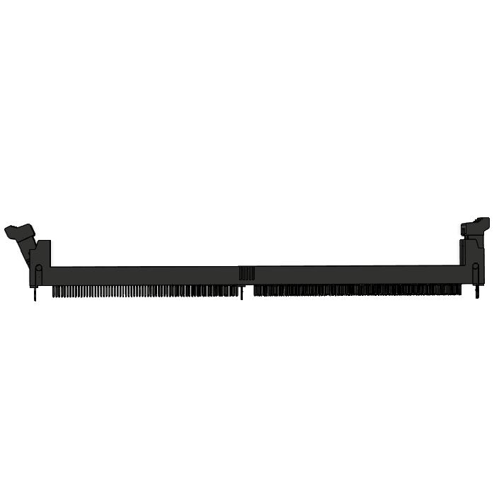
Selecting the right socket requires a multidimensional engineering approach. You must evaluate electrical, mechanical, and environmental specifications simultaneously. A failure in any single dimension compromises the entire memory subsystem.
You must verify bandwidth and data rate support first. Check the manufacturer's S-parameter data. Ensure the socket rates for the maximum MT/s of your intended memory module. Using a socket rated for 4800 MT/s in a 6400 MT/s system causes immediate signal degradation. You will see closed eye diagrams and high error rates on your oscilloscope. Always match the socket bandwidth to your system architecture. Request the Touchstone (.s4p) files from the vendor to run your own channel simulations.
Evaluate impedance and insertion loss rigorously. The socket must meet target impedance specifications. This typically means 50 ohms for single-ended signals and 100 ohms for differential pairs. Minimal signal attenuation is critical. Review the return loss graphs provided by the vendor. High return loss indicates impedance mismatches within the contact geometry. These mismatches reflect energy back toward the transmitter, destroying signal integrity. Look for insertion loss curves that remain flat well beyond the Nyquist frequency of your target data rate.
Assess per-contact current and voltage ratings carefully. This matters immensely for DDR5 architectures. The 5V input pins carry significant current to feed the on-module PMIC. Exceeding the current rating causes localized heating. Over time, this degrades the contact plating and weakens the plastic housing. Ruggedized applications also demand higher voltage safety margins to prevent arcing in low-pressure environments, such as high-altitude aerospace applications.
Mounting styles dictate your manufacturing process. Surface Mount Technology (SMT) dominates high-speed designs. It minimizes stub lengths, improving signal integrity. Plated Through-Hole (PTH) offers superior mechanical strength. However, PTH creates signal stubs that ruin high-frequency performance unless you back-drill the PCB. Press-Fit connectors avoid soldering entirely. They work well for thick backplanes but require specialized insertion tooling. Choose the style that balances your signal requirements with manufacturing capabilities.
Evaluate rack density and form factor constraints early in the design phase. Connector height impacts airflow in 1U and 2U server chassis. Pitch spacing determines how many modules fit on the board. Ejector styles matter too. Standard ejectors require clearance at the ends of the socket. Low-profile ejectors save space but make module removal difficult for field technicians. Maximize your memory density without choking system airflow or blocking adjacent PCIe slots.
Analyze mating cycles and contact plating. Standard consumer sockets use 15µ" gold plating. They guarantee roughly 25 insertion cycles. Enterprise and industrial sockets use 30µ" gold plating. They survive 100 or more cycles. Thicker plating prevents fretting corrosion. It maintains low contact resistance over the product's lifespan. Never skimp on plating thickness for hardware requiring frequent upgrades or maintenance.
Table 3: Contact Plating Thickness vs. Application
Plating Thickness | Guaranteed Mating Cycles | Target Application | Corrosion Resistance |
|---|---|---|---|
Gold Flash (1-3µ") | < 10 Cycles | Disposable Consumer Electronics | Low |
15µ" Gold | 25 Cycles | Standard Desktops, Laptops | Moderate |
30µ" Gold | 100+ Cycles | Enterprise Servers, Industrial PCs | High |
50µ" Gold | 200+ Cycles | Military, Aerospace, Test Fixtures | Extreme |
Operating temperature ranges dictate material selection. The connector plastics must withstand reflow soldering temperatures. Liquid Crystal Polymer (LCP) handles 260°C reflow profiles without warping. It also survives high operational thermal loads. Standard polyamides may blister or deform during assembly. Ensure your chosen socket matches your factory's thermal profile. Warped plastics lead to lifted pins and immediate manufacturing defects.
Review shock and vibration tolerance standards. Applications subject to continuous mechanical stress require certified components. Look for compliance with MIL-STD-810 or EIA-364 testing standards. These tests simulate years of vibration in hours. A certified socket maintains electrical continuity during severe shock events. Uncertified sockets will experience micro-interruptions. A micro-interruption lasting just a few nanoseconds will crash the operating system instantly.
Consider outgassing and contamination risks. Vacuum environments pull volatile compounds out of cheap plastics. This outgassing condenses on nearby optical sensors or sensitive electronics. Clean-room applications require low-outgassing materials. Verify the material safety data sheet (MSDS) for the connector housing. Ensure it meets your specific environmental cleanliness standards before integrating it into satellite or medical imaging hardware.
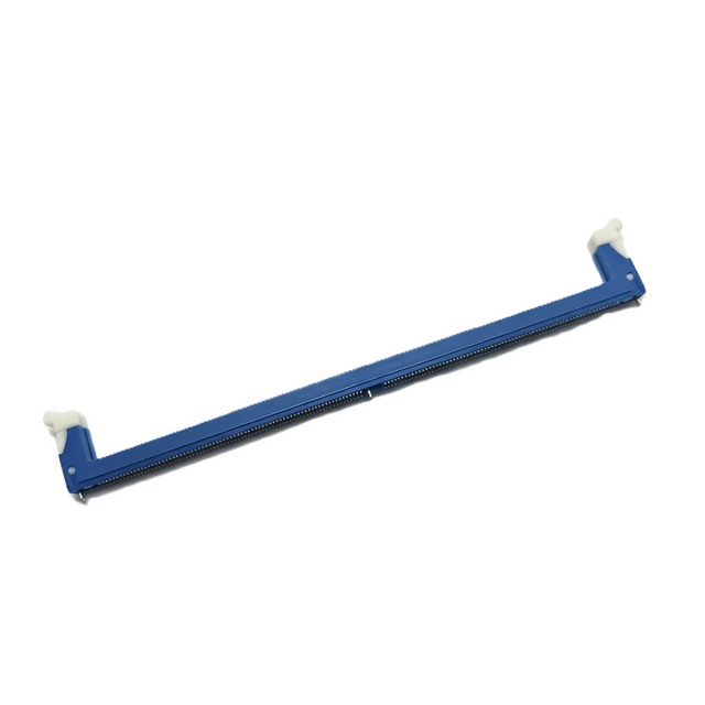
A premium DDR Connector cannot fix a terrible PCB layout. You must co-design the board and socket as a single high-frequency system. The interface between the socket pads and the PCB traces represents the highest risk area for signal degradation.
Routing and layout challenges dominate memory design. You must route high-speed traces out of the connector footprint carefully. Minimize stub lengths at all costs. Impedance discontinuities at the socket breakout region ruin signal integrity. Keep trace lengths matched within tight tolerances. Follow these specific routing practices to mitigate signal loss:
Route high-speed memory traces on inner PCB layers to utilize stripline configurations, reducing EMI radiation.
Back-drill all through-hole vias associated with the memory socket to eliminate resonant stubs.
Maintain a minimum of 3W spacing between aggressive signal traces to prevent cross-coupling.
Ensure solid, uninterrupted ground reference planes directly above and below the memory routing layers.
Match the trace lengths of all signals within a specific byte lane to within 10 mils to ensure timing margins.
Crosstalk mitigation requires strict attention. Near-End Crosstalk (NEXT) and Far-End Crosstalk (FEXT) degrade data lines. Manage coupling within the connector pinout. The immediate PCB breakout region is highly susceptible to crosstalk. Maintain proper spacing between aggressive signals and sensitive receivers. Use ground vias strategically to isolate signal groups. Follow the connector manufacturer's recommended footprint exactly. Do not alter pad sizes or via placements without running full 3D electromagnetic simulations.
Electrical verification prevents mass production disasters. Utilize DDR interposers to probe signals directly at the socket. Connect these interposers to high-bandwidth oscilloscopes. Validate signal integrity under real-world loads. Ensure strict JEDEC compliance before signing off on the design. Simulation software helps, but physical verification catches hidden layout flaws. You must verify the read/write eye diagrams across all temperature extremes.
Thermal management is increasingly difficult. High-density memory modules generate massive heat. The DDR5 PMIC concentrates this heat near the socket. Ensure the connector material does not warp under sustained thermal loads. Warpage lifts pins off the PCB pads, breaking connections. Design your board layout to route airflow directly over the memory banks. Consider the mechanical interference between the socket ejector latches and any aftermarket memory heatsinks.
Manufacturing yield risks plague high-pin-count devices. Coplanarity issues during SMT reflow cause open circuits. A 288-pin socket must sit perfectly flat on the solder paste. If the plastic housing warps during heating, the middle pins lift. Specify a maximum coplanarity deviation of 0.1mm. Work closely with your assembly house to optimize the thermal profile for large memory sockets. Inspect the first article boards using 3D X-ray to verify solder joint integrity under the socket housing.
Procurement decisions impact the entire product lifecycle. You must balance engineering requirements with supply chain realities. Selecting a highly specialized socket might solve a technical challenge but create a massive bottleneck during mass production.
Component selection presents a constant trade-off. Premium features like 30µ" gold plating and high-temperature LCP plastics increase the bill of materials. High-volume consumer devices often cannot support these premiums. You must determine the absolute minimum viable specification for your application. Do not over-engineer a disposable consumer product. Conversely, do not under-engineer a medical device. Match the component specifications directly to the expected operational lifespan and failure impact of the final product.
Evaluate lifecycle and availability guarantees. Industrial and medical designs often stay in production for a decade. You need a manufacturer who guarantees long-term availability. Premature obsolescence forces costly board redesigns and recertification cycles. Ask vendors for their product lifecycle roadmaps. Avoid proprietary sockets unless absolutely necessary for performance. Stick to standard JEDEC form factors to ensure long-term viability.
Second-sourcing mitigates severe supply chain disruptions. Select standard JEDEC footprints whenever possible. Standard footprints allow for drop-in replacements from multiple connector vendors. If your primary supplier faces a factory shutdown, you can pivot immediately. Proprietary footprints lock you into a single vendor. This creates unacceptable risk for high-volume manufacturing lines. Always qualify at least two vendors for your memory sockets during the initial design phase.
The selection of a memory socket remains a critical engineering choice. This choice dictates the upper limits of your system's performance and reliability. Treating it as an afterthought guarantees field failures and degraded throughput. You must approach this component with the same rigor applied to the CPU and memory modules themselves. Base your final selection on a strict evaluation matrix prioritizing JEDEC generation compatibility, mechanical footprint constraints, environmental ruggedness, and signal integrity margins.
With 20 years of experience focused on precision connector technology, CONSHARE integrates connector design, development, production, and sales to support customers with reliable interconnection solutions. Its technical and manufacturing capabilities provide additional support for projects requiring stable connector performance and customized solutions.
Download S-parameter models and 3D CAD files from shortlisted vendors to run preliminary channel simulations.
Procure physical samples of the sockets to perform mechanical fit checks and thermal cycle testing in your lab.
Design a prototype evaluation board to verify routing breakout strategies and measure actual insertion loss.
Validate full JEDEC compliance using an interposer and high-bandwidth oscilloscope before approving the final bill of materials.
A: No. While both standard DIMMs feature 288 pins, the alignment key sits in a different position. This mechanical barrier prevents incorrect insertion. The electrical pinouts and power delivery architectures also differ entirely. Forcing a module into the wrong socket causes immediate physical damage to both the board and the memory stick.
A: Surface Mount Technology (SMT) solders pins directly to the board surface, offering superior high-frequency signal integrity by eliminating via stubs. Plated Through-Hole (PTH) pins pass through the board, providing stronger mechanical retention but creating signal reflections that degrade high-speed data transmission unless the PCB is back-drilled.
A: Gold plating prevents oxidation and fretting corrosion on the contacts. Standard 15µ" plating typically supports around 25 insertion cycles, suitable for consumer electronics. Industrial applications use 30µ" plating, which withstands over 100 cycles and maintains low contact resistance in harsh, vibrating environments.
A: DDR5 architecture moves the Power Management IC (PMIC) from the motherboard directly onto the memory module. The motherboard supplies 5V to the socket, and the PMIC steps it down. This localized power conversion generates significant heat directly above the connector, requiring high-temperature plastics to prevent warpage.
A: Standard plastic latches generally fail under heavy, continuous vibration. The mass of the memory module acts as a pendulum, wearing down the electrical contacts. For high-vibration environments, you should specify ruggedized sockets with metal-reinforced ejectors or specialized screw-down retention mechanisms.
A: Coplanarity issues occur when the plastic housing of a large, high-pin-count socket warps during the intense heat of the SMT reflow oven. If the housing bows, the center pins lift off the solder paste, resulting in open circuits. Using high-temperature LCP plastics mitigates this risk.


