
Views: 0 Author: Site Editor Publish Time: 2026-08-31 Origin: Site


Interconnect failures disproportionately impact overall system reliability across electronic hardware. Connector selection often becomes a late-stage design bottleneck. This oversight forces costly printed circuit board (PCB) respins and delays product launches. Engineering teams constantly face the tension between shrinking PCB real estate, which drives the need for finer pitches, and the uncompromising demand for higher current density, flawless signal integrity, and mechanical robustness in harsh environments. Solving this challenge requires moving away from ad-hoc component selection. Hardware designers must adopt a systematic evaluation framework for specifying a Board to Board Connector based on strict spatial constraints, rigorous electrical requirements, and actual manufacturing realities. Balancing these dimensions ensures long-term field reliability, minimizes assembly defects, and maintains signal fidelity under thermal and mechanical stress.
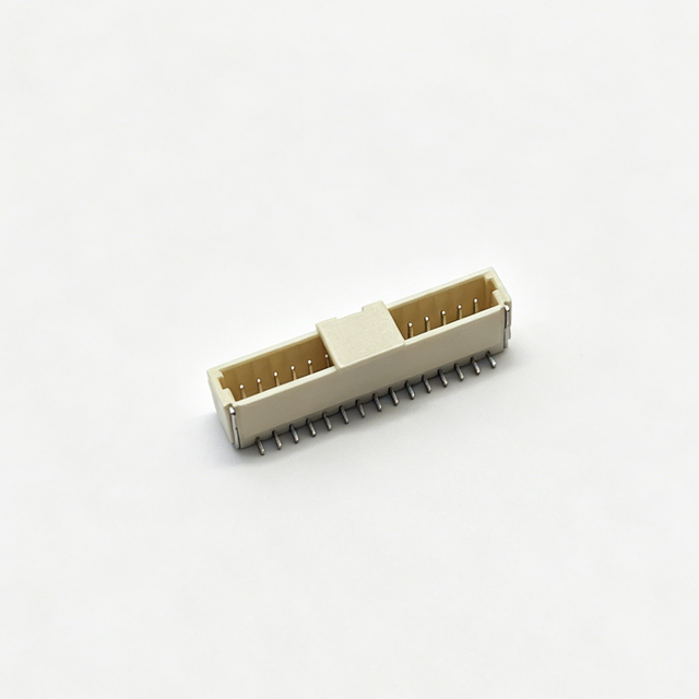
Spatial vs. Electrical Trade-offs: Selecting connector pitch (e.g., 0.4mm to 2.54mm) dictates not only PCB footprint but also maximum current carrying capacity and signal isolation.
Orientation Dictates Architecture: The choice between mezzanine (parallel), coplanar (edge-to-edge), and orthogonal (perpendicular) connectors fundamentally drives the device's thermal and mechanical enclosure design.
BOM and Assembly Efficiency: Utilizing rigid board to board connectors over wire-to-board alternatives reduces manual assembly labor, while hermaphroditic (genderless) designs can streamline inventory.
Manufacturing Realities: Fine-pitch surface mount (SMT) connectors require strict coplanarity controls and alignment features to prevent blind-mating damage during assembly.
Application-Specific Shielding: Industry 4.0 and high-speed telecom applications increasingly require shielded, impedance-matched connectors to mitigate electromagnetic interference (EMI) and crosstalk.
Table of Contents
Evaluating when to eliminate cable assemblies in favor of rigid paired connector systems is the first step in interconnect architecture. Wire-to-board solutions introduce manual assembly labor, increase the risk of routing errors, and add parasitic inductance through the cable length. Rigid paired systems eliminate these variables. They lower parasitic inductance, improve spatial efficiency within tight enclosures, and allow for automated pick-and-place assembly. Engineers specify rigid connections when spatial predictability and high-frequency signal integrity outweigh the need for flexible routing. We see this shift heavily in dense server racks and compact industrial controllers where every millimeter counts. Furthermore, eliminating cables removes the risk of wire chafing against metal enclosures during high-vibration events, a common failure mode in heavy machinery.
Establishing the hard limits for X, Y, and Z axes prevents late-stage mechanical interference. Designers must define the required stacking heights and the allowable tolerances for board-to-board spacing. The Z-axis tolerance stack-up includes the PCB thickness, solder paste thickness, and the plastic housing dimensions of the connector itself. Failing to account for these combined tolerances leads to incomplete mating, reduced contact wipe, and eventual open circuits under vibration. You must calculate the worst-case scenario for these tolerances. If the combined stack-up pushes the connector past its maximum reliable mating depth, the contacts will barely touch. This creates high resistance joints that generate heat and eventually fail. Mechanical engineers must also account for the insertion and extraction forces required. High pin-count connectors can require significant force to mate, sometimes necessitating mechanical assist levers or heavy-duty board stiffeners to prevent the PCB from bowing during assembly.
Electrical baselines dictate the physical size and material composition of the contacts. Engineers determine the required current per pin by applying strict derating curves for expected operating temperatures. High ambient temperatures reduce the current-carrying capacity of the copper alloy contacts. You cannot simply read the datasheet maximum and apply it to a 105°C environment. A contact rated for 3 Amps at room temperature might safely carry only 1.5 Amps at elevated temperatures. Furthermore, designers must calculate necessary voltage clearances based on industry standards. Creepage and clearance distances prevent electrical arcing between adjacent pins, especially in high-voltage industrial or automotive applications. If you run 400V across a 0.5mm pitch without proper conformal coating or isolation slots, you will get arcing. Engineers must also factor in the dielectric withstanding voltage of the plastic housing material, ensuring it can handle transient voltage spikes without breaking down.
Routing high-speed digital or RF signals through an interconnect requires treating the connector as a transmission line. Engineers evaluate insertion loss, return loss, and impedance matching to maintain signal fidelity. Mismatched impedance at the connector interface causes signal reflections, degrading the eye diagram in high-speed data streams. Connectors specified for gigabit protocols must feature optimized contact geometries and appropriate grounding structures to minimize crosstalk between adjacent differential pairs. We often use dedicated ground pins flanking every high-speed differential pair to contain the electromagnetic field and prevent aggressive signal coupling. Testing these parameters requires vector network analyzers to measure S-parameters across the intended frequency band. A connector that performs perfectly at 1 GHz might exhibit severe resonance and signal degradation at 10 GHz due to its internal stub lengths.
Field reliability depends entirely on matching the connector specifications to the deployment environment. Success criteria include defining operating temperature ranges, expected mating cycles, and exposure to shock or vibration. Connectors in modular devices require high mating cycle ratings, utilizing thicker gold plating on the contact surfaces. Standard flash gold will wear off after 50 cycles, exposing the nickel underplate to oxidation. High-reliability applications often specify 30 microinches or more of hard gold plating. Regulatory standards also dictate material choices. Components must meet RoHS compliance, UL flammability ratings (such as UL94V-0), and automotive AEC-Q qualifications where applicable. For equipment deployed in corrosive environments, engineers must specify contacts with specialized plating to resist sulfur or salt fog exposure, preventing the buildup of insulating oxide layers on the mating surfaces.
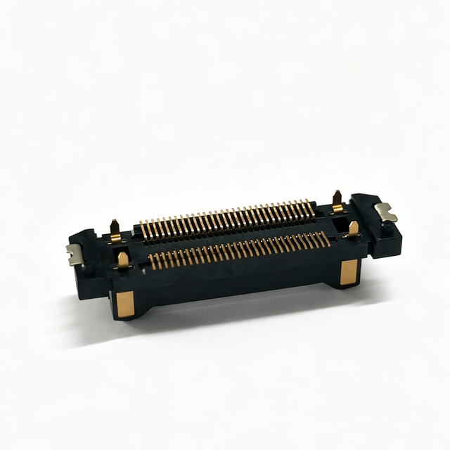
Mezzanine connectors facilitate parallel PCB stacking, creating vertical electrical connections between two or more boards. This architecture stacks boards directly on top of one another, minimizing the horizontal footprint of the overall assembly. Engineers rely on mezzanine configurations for high-density pin counts in compact vertical spaces. Common use cases include System-on-Module (SOM) to carrier board connections and multi-board daisy-chaining in PC/104 architectures.
Despite their spatial efficiency, mezzanine architectures introduce specific limitations. Tightly stacked boards restrict airflow, creating severe thermal management challenges for high-power components trapped between the PCBs. Heat gets trapped in the dead air space. Additionally, testing and probing sandwiched components during prototyping or quality assurance becomes highly difficult, often requiring specialized breakout boards just to verify signal integrity. When designing mezzanine stacks, engineers must carefully map out the thermal dissipation paths, often relying on heavy copper planes within the PCB to wick heat away from the trapped components toward the outer edges of the board.
Coplanar connectors mate two PCBs on the same plane, extending boards horizontally. This architecture utilizes right-angle headers and receptacles mounted at the edge of the PCB. Hardware teams deploy coplanar configurations in applications requiring long, continuous strips of circuitry. Typical use cases include LED lighting arrays, backplane extensions, and modular sensor strips where vertical space is completely restricted.
The primary limitation of edge-to-edge mating is mechanical stress. The connector joints bear the brunt of any bending or flexing across the extended PCB assembly. Engineers must analyze the mechanical stress placed on the PCB edge and often implement supplementary mechanical retention, such as mounting brackets or heavy-duty solder hold-downs, to prevent the pads from tearing off the FR4 substrate. In long LED arrays, thermal expansion of the boards can also push and pull on these coplanar joints, requiring connectors with a degree of longitudinal slide tolerance to absorb the movement without fracturing the solder.
Perpendicular architectures utilize right-angle to vertical mating systems to connect boards at a 90-degree angle. This configuration forms the backbone of traditional motherboard-to-daughterboard designs, often utilizing PCIe or custom backplane architectures. Engineers integrate perpendicular connections in industrial controllers, server racks, and modular test equipment where expansion cards must plug into a central routing hub.
While excellent for modularity, perpendicular mating impacts overall enclosure height significantly. The 90-degree orientation also creates a lever-action effect during physical shock or vibration. This leverage multiplies the stress on the right-angle solder joints, requiring robust through-hole mounting pegs or screw-down hardware to secure the connector housing to the PCB. Designers must also consider the routing complexity on the backplane side, as high-density perpendicular connectors force hundreds of traces to converge into a very narrow routing channel, often requiring 12-layer or 16-layer PCBs to successfully break out all the signals.
Connector Orientation Comparison
Orientation Type | Primary Architecture | Ideal Use Case | Key Limitation |
|---|---|---|---|
Mezzanine | Parallel Stacking (Vertical) | SOM to Carrier, High-Density | Restricted airflow, difficult probing |
Coplanar | Edge-to-Edge (Horizontal) | LED Arrays, Sensor Strips | High mechanical stress on PCB edges |
Perpendicular | Orthogonal (90-Degree) | Backplanes, Expansion Cards | Lever-action stress on solder joints |
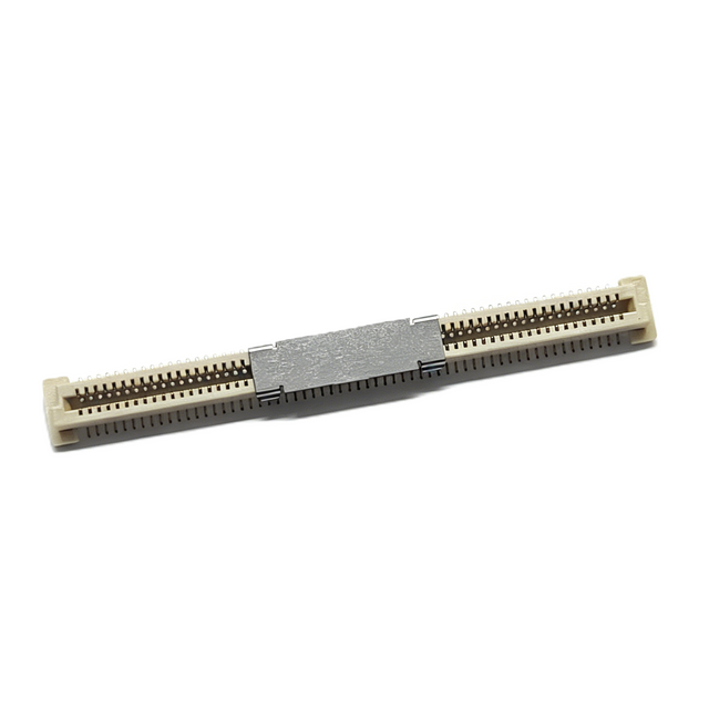
Pitch is the exact measurement from the center of one contact to the center of the next. This single metric dictates the overall connector length, the required PCB footprint, and the trace routing density. Selecting the correct pitch requires balancing miniaturization goals against manufacturing capabilities.
Sub-1.0mm pitch (fine pitch) connectors dominate mobile, wearable, and compact medical devices. They offer massive space savings but demand strict manufacturing tolerances. The fragile pins are highly susceptible to damage during automated pick-and-place assembly and manual handling. Solder paste stencil design becomes highly critical here to prevent bridging between pads. Engineers must specify precise stencil thicknesses and aperture modifications to ensure the correct volume of paste is deposited.
The 1.27mm to 2.00mm pitch range serves as the standard for balancing moderate density with robust mechanical stability. This range is ideal for standard industrial applications, offering enough spacing for reliable solder paste application while maintaining a reasonable footprint. You can route traces between pads much easier at this scale, reducing the need for expensive microvias or high-layer-count boards.
Pitches of 2.54mm and above remain critical for specific engineering requirements. Designers evaluate the use of larger pitches for high-power transmission, high-voltage isolation, and legacy system compatibility where older backplanes are still in service. The larger physical separation naturally increases creepage distances, making them safer for power delivery. These larger connectors also utilize thicker contact beams, providing higher normal force and better resistance to vibration-induced fretting.
Connector Pitch Characteristics and Applications
Pitch Range | Typical Current Rating | Manufacturing Complexity | Primary Application |
|---|---|---|---|
Sub-1.0mm (Fine Pitch) | 0.3A to 1.0A | High (Requires strict stencil control) | Mobile, Wearables, IoT |
1.0mm to 1.27mm | 1.0A to 2.0A | Moderate | Embedded Systems, Sensors |
1.5mm to 2.0mm | 2.0A to 3.0A | Low | Industrial Controllers, Automotive |
2.54mm and Above | 3.0A to 10.0A+ | Very Low | Power Distribution, Legacy Backplanes |
Pin count requirements directly influence row density. Engineers must assess the required number of signals against the available PCB edge space and trace routing complexity. Single-row connectors simplify routing but consume more edge length. Dual-row and multi-row configurations condense the footprint but require complex, multi-layer PCB routing with vias to access the inner rows of pins. When routing high-speed signals out of a multi-row connector, designers must carefully manage via stubs and layer transitions to prevent impedance discontinuities.
Gender configuration also impacts the supply chain and assembly process. Traditional paired systems require stocking both header (male) and receptacle (female) components. Conversely, engineers can specify genderless (hermaphroditic) Board to Board Connector designs. Hermaphroditic connectors mate with themselves, which reduces Bill of Materials complexity, cuts inventory tracking efforts in half, and eliminates the risk of mating the wrong genders on the assembly line. This approach is highly beneficial in modular systems where multiple identical boards need to be daisy-chained together without worrying about male/female orientation.
Stacking height defines the distance between two parallel boards in a mezzanine configuration. Standard stacking heights range from 8mm to 13.8mm, providing adequate space for standard surface-mount components between the boards. Ultra-low profile options exist for smartphones and tablets, bringing the boards within millimeters of each other.
Engineers must calculate the accumulated tolerances of the PCB thickness, solder paste thickness, and connector plastic housing. If the tolerance stack-up exceeds the connector's allowable mating depth, the contacts will not achieve reliable wipe, leading to intermittent electrical failures. Furthermore, stacking height heavily impacts thermal dynamics. Tighter stacking heights restrict airflow between boards, dictating the selection of low-profile thermal interface materials and forcing heat dissipation through the copper planes rather than convection. You must also consider the height of decoupling capacitors and power inductors placed near the connector; a miscalculation in stacking height will cause these components to crash into the opposing board during assembly.
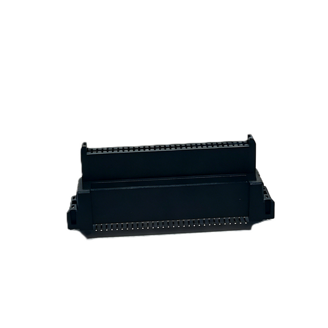
Industrial machinery subjects electronics to continuous, aggressive vibration. Standard rigid connectors often fail under these conditions due to micro-fretting corrosion and solder joint fatigue. Engineers evaluate the necessity of dual-beam contact designs, which provide two points of electrical contact per pin, ensuring continuity even if one beam momentarily lifts during a shock event. This redundancy is non-negotiable for motor drives and robotic controllers.
To combat severe vibration, designers implement floating Board to Board Connector mechanisms. These specialized housings feature an internal spring-like structure that absorbs X, Y, and Z axis misalignments. By allowing the connector interface to move independently of the soldered base, floating connectors prevent mechanical stress from transferring to the solder joints, eliminating the risk of fracturing in heavy machinery. They also compensate for assembly tolerances when multiple rigid connectors are used to mate the same two boards, preventing the boards from bowing under the stress of misaligned pins.
Telecommunications equipment and high-performance computing demand flawless signal integrity at multi-gigabit speeds. Connectors in these applications are no longer just mechanical bridges; they are tuned RF components. Engineers detail the requirement for connectors designed with specific differential pair routing, maintaining strict 85Ω or 100Ω impedance targets through the mating interface to prevent signal reflection. The plastic housing materials must have a low dielectric constant to minimize signal loss at high frequencies.
EMI and crosstalk present massive risks in high-speed data transmission. Designers evaluate the use of integral ground planes within the connector housing to isolate signal pairs. Full metal shielding around the connector exterior is often required to contain emissions and protect sensitive internal routing from external electromagnetic interference generated by nearby power supplies or antennas. In 112G PAM4 applications, even the shape of the contact wipe area is optimized to reduce parasitic capacitance.
Internet of Things (IoT) devices and consumer electronics prioritize absolute miniaturization. Hardware teams assess the trade-offs of ultra-low-profile rigid connectors versus Flexible Printed Circuit (FPC) alternatives. While FPCs offer routing flexibility, rigid fine-pitch connectors provide superior automated assembly speeds and lower component costs at high volumes. Rigid connectors also offer better tactile feedback during manual assembly, reducing the chance of operators partially seating the connection.
Durability remains a critical lens for consumer devices. Engineers evaluate the required mating cycles for devices that may require modular battery replacements, sensor upgrades, or diagnostic access. Connectors subjected to frequent consumer handling require thicker gold plating and robust plastic lead-in chamfers to survive repeated insertion cycles without contact degradation. We also look for connectors with built-in friction locks to prevent the boards from separating if the consumer drops the device.
Blind mating occurs when operators or automated systems assemble two boards without a direct line of sight to the connector interface. This introduces a severe risk of bent pins and crushed plastic housings if the boards are misaligned during insertion. To mitigate this risk, engineers must specify connectors equipped with generous lead-in chamfers. These angled plastic guides physically force the mating halves into alignment before the metal contacts engage. Additionally, utilizing polarizing keys and heavy-duty alignment pegs ensures the boards can only mate in the correct orientation, preventing catastrophic short circuits. In heavy rack-mounted equipment, guide pins on the chassis itself should engage before the connector housings touch, taking the mechanical load off the fragile plastic components.
Surface mount technology relies on all connector pins sitting perfectly flat against the PCB pads. The risk of open circuits increases dramatically if the connector housing warps during the high temperatures of reflow soldering. Engineers mitigate this by mandating strict coplanarity specifications, typically requiring all pins to align within a tolerance of less than 0.1mm. To protect the fragile SMT joints from mechanical strain during mating and unmating, designers evaluate the use of hold-down tabs (solder nails). These metal brackets solder directly to the PCB ground plane, transferring mechanical forces away from the signal pins and into the board substrate. Post-reflow inspection is also critical; Automated Optical Inspection (AOI) and X-Ray systems must be used to verify that solder has properly wicked up the heel and toe of every hidden pin under the connector body.
Rigid board assemblies subjected to extreme thermal cycling face the risk of shear stress. The PCB substrate (typically FR4) and the connector's plastic housing (often Liquid Crystal Polymer) expand and contract at different rates when heated. Over thousands of thermal cycles, this Coefficient of Thermal Expansion (CTE) mismatch applies severe shear stress to the solder joints, eventually causing them to crack. Engineers mitigate CTE risks by utilizing flexible interconnects for wide temperature variations or deploying floating connector designs that absorb the thermal expansion differentials without stressing the solder bonds. Selecting housing materials with a CTE closely matched to FR4 is another effective strategy for high-reliability aerospace or automotive applications.
Define hard spatial constraints by locking in the required pitch, stack height, orientation, and row density based on the mechanical enclosure limits.
Filter the shortlisted options by electrical requirements to ensure the contacts meet current derating curves, voltage clearances, and high-speed impedance targets.
Verify manufacturing tolerances by calculating the Z-axis stack-up and confirming the selected housing materials withstand the intended SMT reflow temperature profiles.
Implement mechanical mitigations like alignment pegs, hold-down tabs, or floating mechanisms to protect solder joints from blind mating damage and operational vibration.
Beyond connector selection criteria, working with a specialized interconnect partner can help simplify component evaluation and reduce sourcing risks. CONSHARE focuses on connector solutions for electronic applications, offering a practical product foundation for engineers developing compact, reliable, and performance-driven PCB systems.
A: The 1.27mm to 2.00mm pitch range is standard for industrial applications. It provides an optimal balance between spatial density and the mechanical robustness required to withstand vibration and repeated handling.
A: Floating connectors feature a spring-like internal housing that allows the mating interface to move independently of the soldered base. This absorbs X, Y, and Z axis misalignments, preventing vibration and thermal expansion stress from fracturing the solder joints.
A: Blind mating damage occurs when operators assemble boards without a clear line of sight, leading to misalignment. If the connectors lack lead-in chamfers or alignment pegs, the forced insertion crushes the plastic housing and bends the metal contacts.
A: Tighter stacking heights severely restrict convective airflow between parallel boards. This traps heat generated by high-power components, requiring engineers to implement low-profile thermal interface materials or route heat through the PCB copper layers.
A: Hermaphroditic connectors are genderless, meaning they mate with themselves. This eliminates the need to source and stock separate male and female components, simplifying the Bill of Materials and reducing the risk of assembly errors.
A: For reliable surface mount assembly, the coplanarity of all connector pins must typically remain under 0.1mm. Exceeding this tolerance prevents pins from making contact with the solder paste, resulting in open circuits after reflow.


