
Views: 0 Author: Site Editor Publish Time: 2026-08-31 Origin: Site


The demand for data throughput in enterprise environments pushes hardware architectures to their physical limits. AI workloads, high-density storage, and 5G networking require massive, uninterrupted bandwidth. Selecting the right interconnects dictates signal integrity, thermal management, and overall system scalability. Suboptimal component selection leads to bottlenecked data rates, excessive heat generation, and premature hardware obsolescence.
This guide provides a technical evaluation framework for specifying a Backplane Connector. We focus on their application in modern servers, blade architectures, storage enclosures, and industrial systems. You will learn how to balance pin density with signal integrity, evaluate mechanical tolerances, and choose the right architectural approach to ensure long-term reliability and peak performance.
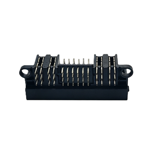
Data Rate Scalability: Modern backplane systems must support multi-gigabit to 112Gbps/224Gbps data rates (often utilizing PAM4 modulation) to future-proof server and storage infrastructure.
Signal Integrity vs. Density: The primary engineering trade-off in backplane design is balancing high-density pin counts with low insertion loss and stringent crosstalk mitigation.
Mechanical Reliability: Robust mating cycles, blind-mate capabilities, and thermal resilience are non-negotiable for enterprise-grade storage clusters and top-of-rack switches requiring hot-swappability.
Architectural Flexibility: Evaluating traditional PCB backplanes against orthogonal and cabled backplane systems is critical for optimizing airflow and reducing trace lengths.
Table of Contents
Modern data centers operate under extreme performance pressures. Legacy board-to-board interconnects act as low-pass filters at high frequencies. They fail to support PCIe Gen 5 and Gen 6 requirements. They cannot sustain 400G or 800G Ethernet speeds. This creates system-wide latency. When high-frequency harmonics are attenuated, the digital eye diagram closes. This results in unacceptable bit error rates (BER). You must select components capable of handling these extreme frequencies without degrading the signal. The physical layer must remain transparent to the data passing through it.
Engineers face a dual requirement during system design. The backplane must act as a rigid mechanical integration plane. Simultaneously, it must manage high-current power distribution alongside sensitive high-speed signals. Mixing power and data in tight proximity introduces electromagnetic interference (EMI) risks. Dedicated power pins must handle high amperage without causing thermal runaway. Signal pins must remain isolated from this power delivery network. Achieving this balance requires precise internal shielding and optimized contact geometries. You cannot compromise one for the other without risking system stability.
Continuous uptime is a strict business requirement for enterprise infrastructure. Hot-swappable components are mandatory. This necessitates highly reliable blind-mating designs. When technicians replace a failed compute blade or storage drive, they cannot see the mating interface. The interconnect must physically guide the module into perfect alignment. Without generous gatherability tolerances, pins will bend. Housings will fracture. A single damaged pin can bring down an entire server node. Mechanical robustness directly translates to system availability.
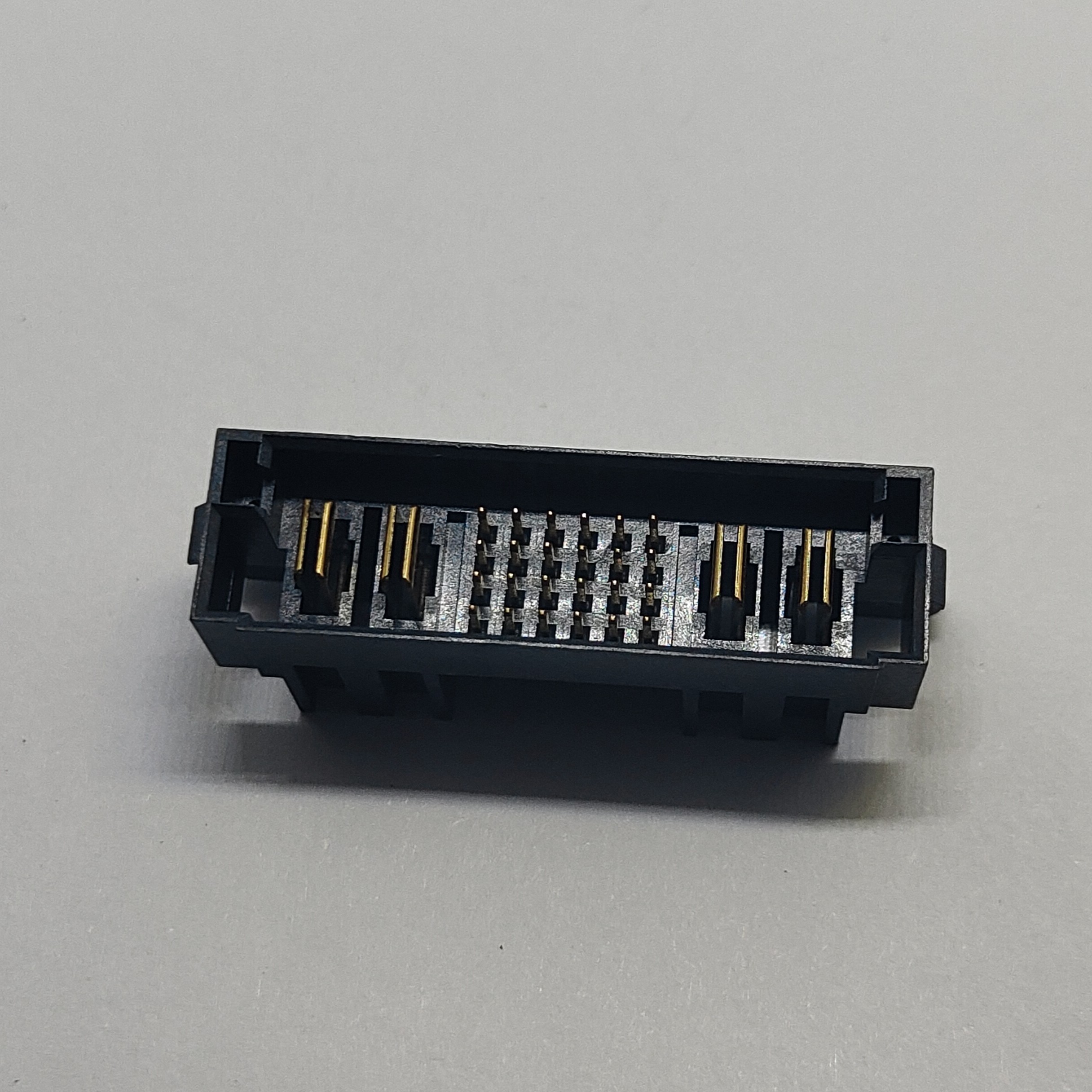
Blade servers maximize compute density within a limited chassis volume. They rely on high-density interconnects to interface compute blades with chassis power and networking fabrics. Space constraints dictate the use of low-profile form factors. Bulky components impede chassis airflow, leading to thermal throttling of CPUs and GPUs. You need solutions that offer maximum differential pairs per square inch while maintaining a minimal vertical profile. Every millimeter of saved space allows for larger heatsinks or additional memory modules.
Power delivery is equally demanding in blade architectures. Modern AI compute nodes draw massive current. The interconnect must distribute hundreds of amps from the chassis power supply to the blade. This requires specialized power contacts integrated alongside the high-speed data arrays. The mechanical housing must withstand the insertion forces of heavy, fully populated compute blades. A fully loaded blade can weigh over twenty pounds, exerting significant shear stress on the mating interface during installation.
Storage architectures vary between hybrid hard drive clusters (JBOD) and all-flash NVMe arrays (JBOF). Hybrid systems routing SAS or SATA signals operate at lower frequencies. They prioritize mechanical durability over extreme signal integrity. All-flash NVMe arrays route PCIe Gen 4 or Gen 5 signals directly to the drives. These require strict impedance control and ultra-low crosstalk. The physical layer must support the massive parallel bandwidth generated by dozens of NVMe drives operating simultaneously.
Storage drives undergo frequent replacements and capacity upgrades. High mating-cycle durability is essential. Standard interconnects may degrade after 50 cycles. Storage backplanes often require ratings of 250 to 500 cycles. Ruggedized housings prevent wear and tear during routine maintenance. Heavy gold plating on the contact wipes ensures reliable connectivity over the hardware's lifespan. Thicker plating prevents the underlying nickel barrier from exposing copper to oxidation after repeated insertions.
Top-of-Rack switches route massive I/O bandwidth between switch line cards and switch fabric cards. A 25.6T or 51.2T switch ASIC requires hundreds of high-speed lanes. The interconnects form the central nervous system of the switch. They must handle dense routing without introducing skew or resonance. Structural rigidity is vital. Heavy line cards exert significant torque on the backplane during insertion and removal. The housing must prevent the contacts from shifting under this mechanical load.
Telecommunications equipment must adhere to strict industry standards. NEBS (Network Equipment-Building System) compliance dictates resistance to earthquakes, fires, and extreme temperatures. Components used in these environments require robust mechanical retention features. They must maintain contact continuity during severe vibration events. Signal loss for even a microsecond can drop thousands of active network sessions. Engineers must specify components with high normal force contacts to guarantee uninterrupted service during seismic activity.
Edge data centers and industrial control systems operate outside climate-controlled environments. Deploying backplane architectures in harsh environments introduces unique challenges. Airborne contaminants, moisture, and corrosive gases attack exposed metal contacts. You must evaluate requirements for extreme vibration resistance and extended operating temperature ranges. Industrial systems often require components rated from -40°C to 85°C. Standard commercial parts will fail rapidly under these conditions.
Conformal coating is frequently applied to industrial PCBs. The interconnect housing must prevent this coating from wicking into the contact interface. Fretting corrosion is a major risk in high-vibration environments. Micro-movements between mated contacts wear away the protective gold plating. This exposes the underlying metal to oxidation. High-normal-force contacts mitigate this risk by maintaining a gas-tight seal during vibration. Lubricated contacts can also extend the lifespan of systems deployed in heavy manufacturing facilities.
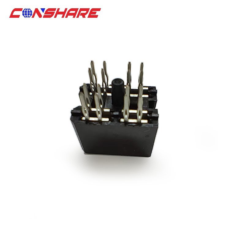
Signal integrity determines the maximum viable data rate of your system. You must map impedance control and shielding features directly to performance outcomes. Sustaining 112G or 224Gbps PAM4 signaling requires mitigating insertion loss and return loss. PAM4 modulation transmits four voltage levels instead of two. This reduces the signal-to-noise ratio margin. Any impedance mismatch at the mating interface causes signal reflections, destroying the data eye. The physical design of the contact must minimize parasitic capacitance and inductance.
Component selection heavily impacts the overall channel loss budget. A typical 112G channel has a strict insertion loss budget at the Nyquist frequency (28 GHz). If the interconnect consumes too much of this budget, the PCB trace lengths must be drastically shortened. You need precise SI simulation data from vendors. You must also ensure synergy with ultra-low loss PCB laminates like Megtron 6 or Megtron 7. The transition from the PCB via to the component pad is often the largest source of impedance discontinuity. Optimizing the via footprint is just as important as selecting the right component.
Engineers constantly battle the trade-off between density and signal integrity. Maximizing differential pairs per square inch allows for smaller chassis designs. However, packing high-speed signals tightly together increases near-end crosstalk (NEXT) and far-end crosstalk (FEXT). Electromagnetic fields couple between adjacent pins. You must evaluate the internal shielding structures. Ground planes or lossy conductive plastics are often used to isolate individual differential pairs. Effective shielding prevents aggressive signals from corrupting adjacent victim channels.
Pitch sizes directly impact PCB routing complexity. A tighter pitch requires narrower trace widths and smaller vias. This increases PCB manufacturing costs and layer counts. A 0.8mm pitch might require a 24-layer board to route all signals out of the connector footprint. A 1.0mm pitch might allow routing on a 16-layer board. You must weigh the component density against the resulting bare board fabrication costs. Sometimes a slightly larger component saves thousands of dollars in PCB manufacturing expenses.
The method used to attach the component to the PCB affects both mechanical strength and high-frequency performance. You must choose the termination style based on board thickness and data rate requirements. Each method presents distinct manufacturing and performance characteristics.
Press-Fit (Compliant Pin): Press-fit terminations dominate thick, high-layer-count backplane PCBs. The compliant pin deforms inside the plated through-hole. This creates a gas-tight, highly reliable mechanical bond. It avoids the thermal stress of wave soldering or SMT reflow on massive, thick PCBs. Thick backplanes act as massive heat sinks, making traditional soldering nearly impossible.
Surface Mount (SMT): SMT or paste-in-hole reflow methods are viable for thinner line cards. SMT eliminates the plated through-hole stub. Vias can be back-drilled or blind, drastically improving signal integrity at extreme frequencies. However, SMT joints lack the mechanical shear strength of press-fit pins. They require additional mounting hardware to survive the insertion forces of heavy modules.
Technical Evaluation Metrics for High-Speed Interconnects
Evaluation Metric | Primary Impact | Design Consideration |
|---|---|---|
Insertion Loss | Signal reach and data rate limit | Requires ultra-low loss dielectrics and optimized contact geometries. |
Crosstalk (NEXT/FEXT) | Bit Error Rate (BER) degradation | Necessitates internal ground shields and optimized pair-to-pair spacing. |
Mating Cycles | Hardware lifespan and maintenance | Requires thicker gold plating (e.g., 30µin) and ruggedized LCP housings. |
Current Rating per Pin | Power delivery and thermal rise | Needs dedicated power blades separated from high-speed signal arrays. |
Dense server racks generate massive amounts of heat. Component bulk directly impacts system cooling and chassis ventilation. A large interconnect acts as a physical wall, blocking airflow from the front chassis fans to the rear exhaust. You must evaluate the aerodynamic profile of the housings. Some designs incorporate venting channels directly through the plastic body to allow air passage. Reducing the physical footprint of the interconnect lowers the static pressure within the chassis, improving overall fan efficiency.
The thermal resistance of housing materials is critical in high-temperature environments. Liquid Crystal Polymer (LCP) is the industry standard. It withstands high operating temperatures without warping or outgassing. If a housing warps under thermal stress, the contact wipe distances change. This can lead to intermittent disconnects or complete signal failure. You must ensure the chosen materials align with your system's maximum thermal envelope. Plastics that absorb moisture can also shift their dielectric constant, altering the impedance profile of the interconnect.
Proprietary designs lock you into a single vendor ecosystem. Review necessary alignments with industry standards. The Open Compute Project (OCP) defines specific form factors and pinouts for modular server architectures. PICMG defines standards for industrial computing platforms like MicroTCA and CompactPCI. Adhering to these standards ensures interoperability. It guarantees that line cards from different manufacturers will mate correctly and communicate reliably over the specified PCIe generations. Standardization reduces engineering overhead and accelerates time to market.
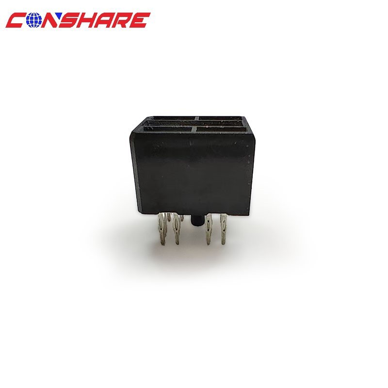
The traditional architecture uses a large, central PCB. Line cards plug into the front. Switch fabric cards or power supplies plug into the rear. Standard PCB-based routing connects the components. This mechanism offers high reliability and relies on proven manufacturing techniques. Power distribution is straightforward using massive copper planes within the board. Hardware engineers have decades of experience designing and troubleshooting these systems.
The primary trade-off is signal degradation and thermal impedance. High-speed signals suffer high insertion loss over long PCB traces. Pushing 112G PAM4 across 20 inches of FR4 material is physically impossible. You must use expensive, exotic PCB laminates. Furthermore, the large vertical board severely restricts front-to-back chassis airflow. This requires more powerful, louder cooling fans. The sheer size of the central board also makes it expensive to manufacture and difficult to replace in the field.
Orthogonal architectures eliminate the central midplane entirely. Vertical line cards connect directly to horizontal fabric cards. The interconnects mate at a 90-degree angle. This mechanism drastically improves front-to-back airflow. Cooling efficiency increases significantly. It also reduces trace lengths to near zero at the mating interface. This provides vastly superior signal integrity compared to traditional routed boards. The elimination of the midplane removes a major point of failure from the system.
The trade-off lies in mechanical complexity. Aligning vertical and horizontal cards requires extreme precision in the chassis sheet metal. Tolerance stack-ups can cause severe mating issues. It also limits modularity. Upgrading a horizontal fabric card requires powering down and removing all intersecting vertical line cards. This architecture is highly performant but difficult to design and maintain. It requires tight collaboration between electrical and mechanical engineering teams during the early design phases.
Cabled systems bypass the PCB entirely for high-speed signal routing. They utilize low-loss twinax cables and hermaphroditic connector designs. The signals travel from the line card ASIC, through a flyover cable, directly to the mating interface. This mechanism enables 224Gbps speeds over much longer distances. It decouples the high-speed data path from the PCB material. You can use cheap standard FR4 for power and low-speed control signals. This hybrid approach optimizes both performance and material costs.
The trade-off is physical volume and assembly complexity. Twinax cables consume significant internal chassis space. Cable management becomes a major engineering challenge. Airflow can be obstructed by dense cable bundles if not routed carefully. Initial component costs are higher than bare PCBs. However, the ability to reach next-generation data rates often justifies the mechanical complexity. Manufacturing these systems requires specialized assembly procedures to ensure cables are not pinched or bent beyond their minimum bend radius.
Unpredictable signal degradation is a massive risk at speeds exceeding 56Gbps. Resonance spikes and impedance mismatches can completely destroy a data channel. A poorly designed via transition or a slight misalignment in the mating interface causes reflections. These reflections bounce back and forth, creating noise that masks the actual data signal. Relying on basic design rules is insufficient for modern high-speed channels.
You must mandate 3D electromagnetic (EM) simulation models from vendors. Do not rely solely on datasheet marketing numbers. Request S-parameter data (Touchstone files) and import them into your channel simulation software. Simulate the entire channel, including the ASIC package, PCB traces, vias, and the interconnect itself. Finalize your PCB layouts only after the simulated eye diagram meets your BER requirements. Follow a strict verification process:
Extract the 3D model of the interconnect and the proposed PCB via footprint.
Run a full-wave EM simulation to generate accurate S-parameters up to 50 GHz.
Import the S-parameters into a system-level channel simulator.
Apply the specific ASIC Tx/Rx equalization settings (FFE, DFE, CTLE).
Analyze the resulting eye diagram for adequate voltage and timing margins.
Hot-swapping heavy modules introduces severe mechanical risks. Pin stubbing occurs when a misaligned pin hits the plastic housing instead of the mating receptacle. Bent contacts or housing fractures cause immediate hardware failure. Tolerance stack-ups in the sheet metal chassis exacerbate these alignment issues. A module might look aligned on the outside but be off by a millimeter at the mating plane. The leverage exerted by a long line card amplifies small misalignments.
Mitigate these risks by specifying components with robust mechanical features. Look for heavy-duty metal guide pins that engage before the electrical contacts. Ensure the housings offer generous gatherability tolerances. Specify ruggedized LCP housings that resist cracking under impact. Conduct extensive mechanical mock-up testing before finalizing the chassis design. Build physical prototypes and perform repeated insertion and extraction cycles to identify potential binding points.
Designing a proprietary architecture around a single-source component is dangerous. If that vendor faces a supply chain disruption, your entire production line halts. If the vendor declares the component end-of-life (EOL), you must redesign your entire system. Enterprise hardware lifecycles often span five to ten years. You need guaranteed component availability for that entire duration. Redesigning a backplane mid-lifecycle is an expensive and disruptive process.
Prioritize components that adhere to multi-source agreements (MSAs). MSAs ensure that multiple independent manufacturers produce mechanically and electrically interchangeable parts. If one vendor fails, you can immediately switch to another. Require vendors to provide established, long-term manufacturing roadmaps. Secure contractual commitments for EOL notifications and last-time-buy opportunities. Maintain active communication with your component suppliers to anticipate market shifts and material shortages.
The optimal Backplane Connector is not universally defined by the highest speed rating. It is defined by the precise alignment of signal integrity, mechanical durability, and architectural constraints. You must balance the electrical demands of next-generation ASICs with the physical realities of chassis airflow and hot-swap mechanics. Your shortlisting logic must reflect your specific application. For AI/ML compute servers, prioritize cabled architectures and 224G-capable twinax solutions to preserve signal integrity. For high-density storage and industrial control systems, prioritize mechanical robustness. Focus on blind-mate gatherability, vibration resistance, and power distribution efficiency.
For engineers evaluating reliable interconnect solutions, CONSHARE brings 20 years of experience in precision connector technology, integrating connector design, development, manufacturing, and sales. With expertise across PCB, PCIe, power, and other high-performance connectivity solutions, CONSHARE supports customers in developing dependable interconnect systems for demanding electronic applications.
Take the following actionable steps to advance your design process:
Request full 3D EM simulation models and S-parameter files from shortlisted vendors to validate your channel loss budgets.
Procure physical evaluation boards to conduct empirical signal integrity testing and verify impedance profiles.
Initiate mechanical tolerance testing by building physical chassis mockups to validate blind-mating gatherability.
Verify multi-source agreement (MSA) compliance to secure your long-term manufacturing supply chain.
A: A backplane interconnect is specifically designed to interface modular plug-in cards with a central rigid backplane. It prioritizes high pin density, robust mechanical alignment for blind-mating, and often integrates high-current power delivery. Standard board-to-board components are typically smaller, handle lower insertion forces, and are used for internal, permanent PCB stacking rather than modular, hot-swappable system architectures.
A: Cabled systems bypass lossy PCB materials entirely. They route high-speed signals through shielded twinax cables directly from the ASIC to the mating interface. This drastically reduces insertion loss and dielectric absorption. It allows servers to achieve 112G and 224G data rates over distances that would be impossible using traditional FR4 or even exotic PCB laminates.
A: State-of-the-art designs currently support 112Gbps per lane using PAM4 modulation. The industry is actively transitioning to support 224Gbps PAM4. Achieving these extreme speeds requires ultra-precise impedance control, advanced internal shielding to eliminate crosstalk, and often necessitates a shift from traditional PCB routing to cabled twinax architectures.
A: An orthogonal architecture eliminates the central midplane. Vertical line cards plug directly into horizontal fabric cards at a 90-degree angle. It should be used in high-performance switches and servers where maximizing front-to-back airflow is mandatory for cooling, and where reducing trace lengths is necessary to meet strict high-speed signal integrity budgets.
A: They utilize hybrid housing designs. Dedicated, heavy-copper power blades are integrated alongside the high-density signal pin arrays. The housings incorporate physical isolation barriers and optimized spacing to prevent electromagnetic interference. This allows a single interconnect block to deliver hundreds of amps of current while simultaneously routing noise-sensitive 112G data signals.
A: Press-fit terminations use a compliant pin that deforms inside a plated through-hole, creating a strong, gas-tight mechanical bond. Backplane PCBs are typically very thick and act as massive heat sinks, making surface-mount reflow soldering highly unreliable. Press-fit avoids thermal stress on the board and provides the necessary shear strength to withstand heavy module insertion forces.


